Amplitude impedance calibrated package interlayer antenna

An impedance calibration, antenna technology, applied in the direction of antenna, radiating element structure, electrical components, etc., can solve the problems of incompatibility, large geometric size, different wave impedance, etc., to achieve the effect of improving consistency

Inactive Publication Date: 2013-04-03
SOUTHEAST UNIV
View PDF2 Cites 4 Cited by
  • Summary
  • Abstract
  • Description
  • Claims
  • Application Information

AI Technical Summary

Benefits of technology

This patented packageized sandwich radar antennas have improved accuracy for measuring waves over different angles without changing their shape or size. They also reduce interference from other sources like background noise caused by nearby objects that may affect them during measurement. Overall, this technology enhances signal quality while reducing unwanted signals outside its intended range.

Problems solved by technology

This patented describes how combining multiple chips together may help reduce signal delays or decrease power consumption when transmitting signals over long distances through wireless communication systems like mobile phones (Mobile Phones). To achieve this, there has developed an improved method called 3D Multi Chickle Assembly (MLA), where both chip packages and external components communicate wirelessly simultanously without adding any extra layers that could make them bigger than usual. By integrating the antennas onto one layer within each other, we aim to enhance its properties while reducing manufacturing costs.

Method used


Image

  • Amplitude impedance calibrated package interlayer antenna
  • Amplitude impedance calibrated package interlayer antenna
  • Amplitude impedance calibrated package interlayer antenna

Examples


Embodiment Construction

[0021] The present invention will be further described below with reference to the drawings and embodiments.

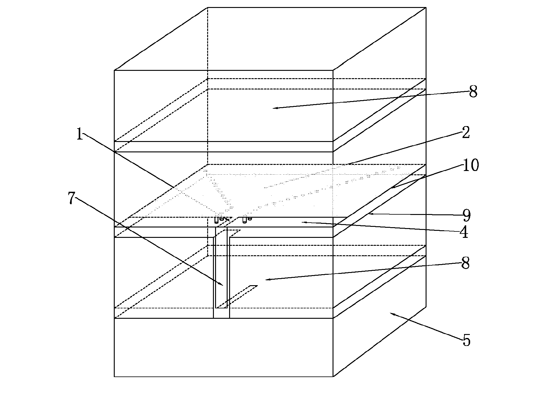
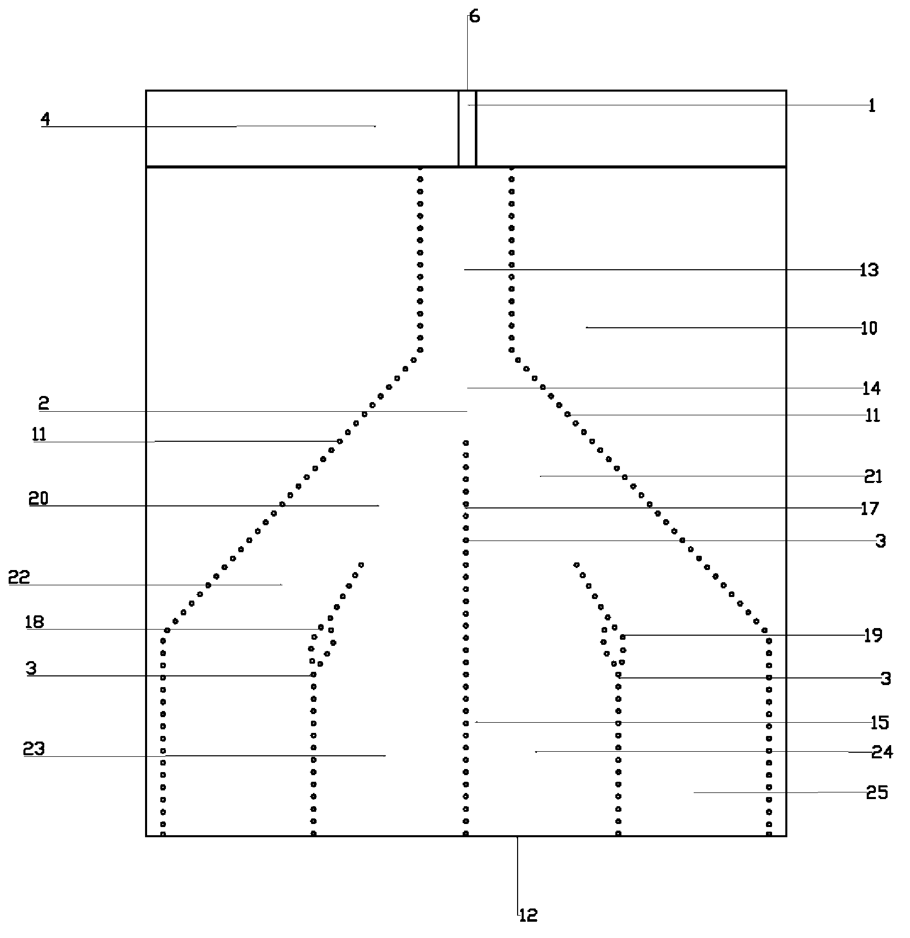
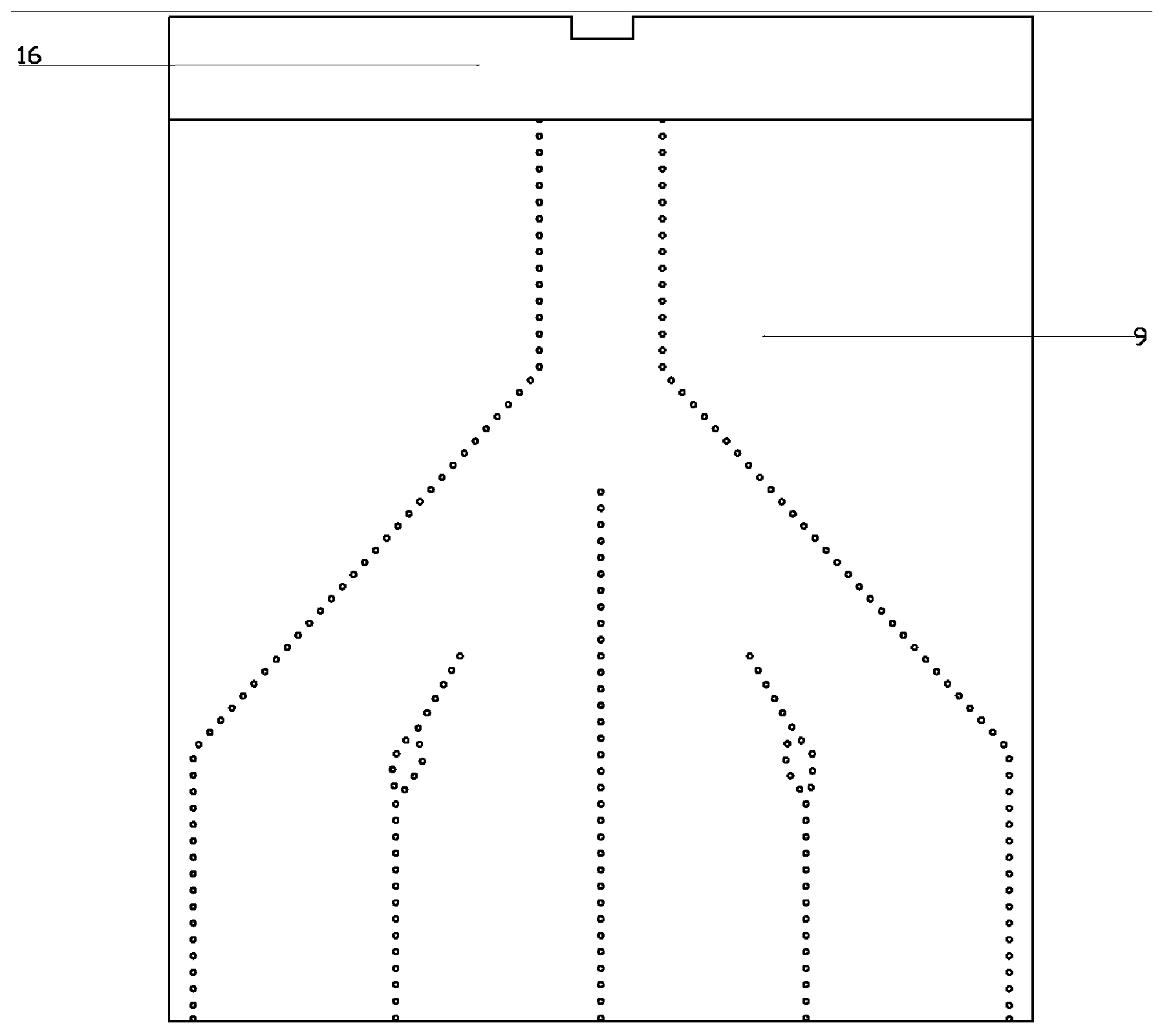
[0022] The implementation adopted by the present invention is: the packaged sandwich antenna with amplitude impedance calibration is composed of three parts: microstrip feeder 1, substrate integrated waveguide horn antenna 2 and embedded metallized via 3, all of which are integrated in the same medium On the substrate 4, the dielectric substrate is located in the inner layer of the 4-dimensional multilayer package 5; one end of the microstrip feeder 1 is connected to the substrate integrated waveguide horn antenna 2, and the other end of the microstrip feeder 1 is close to the side of the package, which is the input and output port 6 of the antenna The input and output port 6 of the antenna is connected to the coplanar waveguide 7 on the side of the package through a 90-degree transition between the microstrip and the coplanar waveguide, and the other end of the coplanar wav


PUM


Abstract

The invention relates to a planar horn antenna, in particular to an amplitude impedance calibrated package interlayer antenna which comprises a micro-strip feeder (1), a horn antenna (2) and metalized via holes (3), wherein the micro-strip feeder (1), the horn antenna (2) and the metalized via holes (3) are integrated on a dielectric substrate (4) which is arranged on the inner layer of a three-dimensional package (5). One end of the micro-strip feeder (1) is connected with an internal circuit (8) through a coplanar waveguide (7) on the lateral side of a package, the horn antenna (2) comprises a bottom metal plane (9), a top metal plane (10) and metalized via side walls (11), a middle metalized via array (17), a left metalized via array (18) and a right metalized via array (19) consist of the metalized via holes (3) and form four dielectric filling waveguides in the horn antenna (2), and port wave impedance of the four dielectric filling waveguides on an antenna caliber surface (12) is equal to free space wave impedance. Antenna caliber efficiency can be improved while return loss is reduced.

Description


Claims


Application Information

Patent Timeline
Owner SOUTHEAST UNIV
Why Eureka
Try Eureka