Driving circuit of optoelectronic equipment and driving method thereof

A technology of optoelectronic equipment and driving circuits, which is applied in the electronic field, can solve the problems that I/O ports cannot complete control tasks, and cannot reduce the occupation of single-chip I/O ports, etc., and achieve the effects of improving reliability, reducing occupancy, and simplifying circuits

Inactive Publication Date: 2012-05-16
SHENZHEN INSTITUTE OF INFORMATION TECHNOLOGY
View PDF5 Cites 16 Cited by
  • Summary
  • Abstract
  • Description
  • Claims
  • Application Information

AI Technical Summary

Benefits of technology

This technology allows an image sensor (CMOS) camera with multiple sensors to communicate over one communication channel without having any extra wires or other components attached to it. Instead, each pixel's color component has its own unique address called gray level code that describes how much light falls on different pixels within the scene being captured during imaging. By converting this signal from analog format to digital form, there are fewer connections needed than traditional methods like connecting cables directly through ports at either ends of the CMOS camera itself. Additionally, these techniques allow for faster processing times due to their ability to process signals quickly instead of relying solely upon external devices such as switches or displays. Overall, they make cameras smarter while improving efficiency and reducing space usage compared to older systems.

Problems solved by technology

Technological Problem: Current OptoElectronics Drive Method (OM) uses fixed connections between segments or individual chips instead of allowing multiple components within one piece of optical material to communicate with each other without interference from external factors like ambient lights. Additionally, current Optroluminescences Display System (OS), where displays images based upon analog voltages applied across electrodes, has limitations due to their complexity.

Method used


Image

  • Driving circuit of optoelectronic equipment and driving method thereof
  • Driving circuit of optoelectronic equipment and driving method thereof
  • Driving circuit of optoelectronic equipment and driving method thereof

Examples


Embodiment Construction

[0022] In order to make the object, technical solution and advantages of the present invention clearer, the present invention will be further described in detail below in conjunction with the accompanying drawings and embodiments. It should be understood that the specific embodiments described here are only used to explain the present invention, not to limit the present invention.

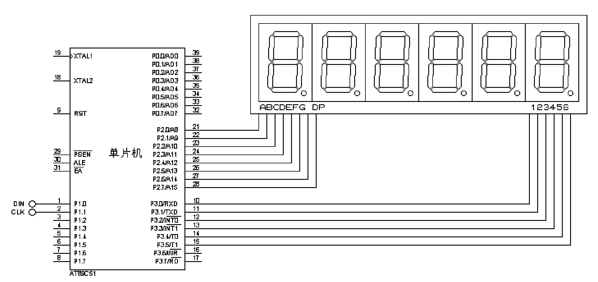
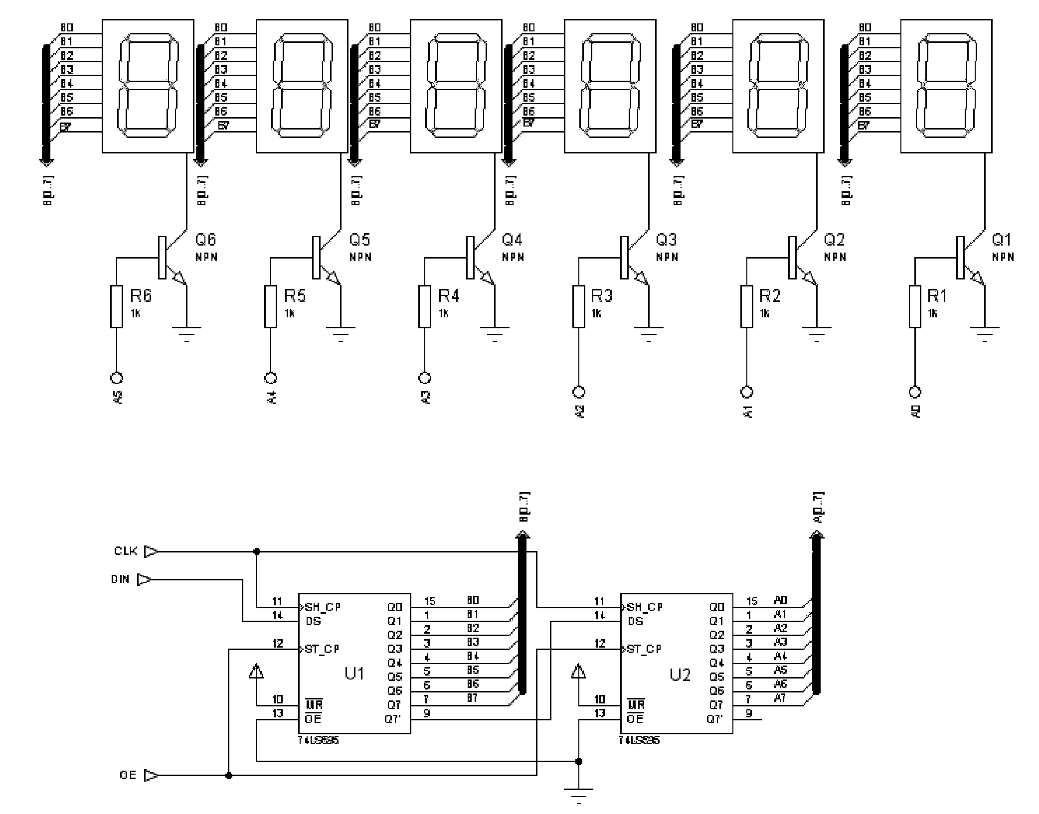
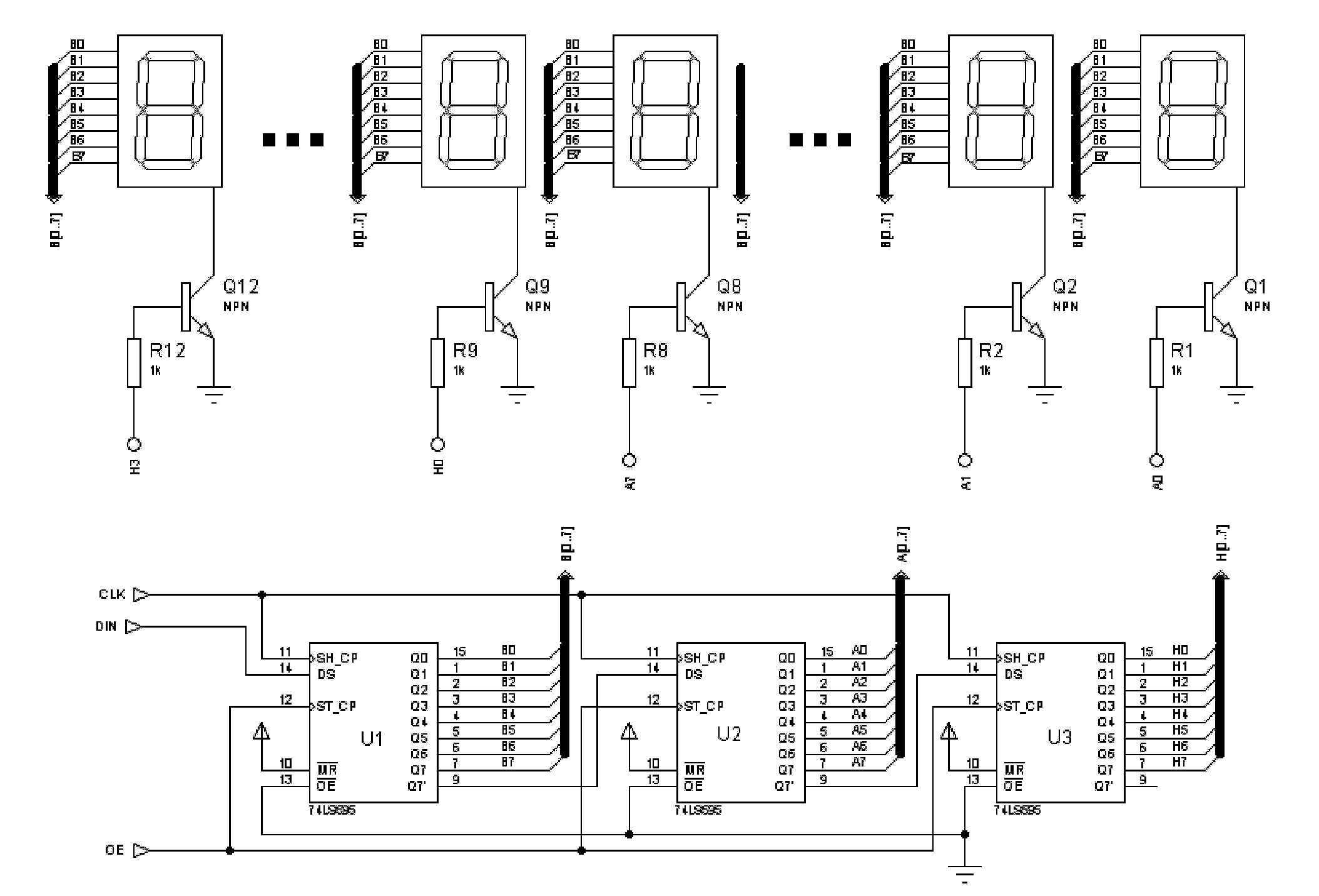
[0023] The invention connects a plurality of serial-to-parallel conversion chips between the single-chip microcomputer and the nixie tube, completes the conversion of data serial-in and parallel-out through the serial-to-parallel conversion chips, and realizes only using three-terminal bus to control and drive the photoelectric equipment.

[0024] figure 2 The driving circuit diagram of the six digital tubes provided for the first embodiment of the present invention only shows the parts related to the present invention for the convenience of description.

[0025] In this embodiment, the drive circui


PUM


Abstract

The invention is suitable for the technical field of electronics and provides a driving circuit of optoelectronic equipment and a driving method thereof. The driving circuit comprises a first series-to-parallel conversion chip and a second series-to-parallel conversion chip, wherein the first series-to-parallel conversion chip is connected with a singlechip through a three-wire bus and is used for converting serial data output by the singlechip into parallel data and outputting the parallel data to the section control end of the optoelectronic equipment; and the second series-to-parallel conversion chip is used for converting the serial data spilled by the first series-to-parallel conversion chip into the parallel data and outputting the parallel data after the conversion to the position gate end of the optoelectronic equipment to control the data of the display section of the optoelectronic equipment. According to the invention, multiple series-to-parallel conversion chips are connected between the singlechip and a digital tube, and the serial-in-parallel-out conversion of data is completed through the series-to-parallel conversion chips, thereby achieving the control of the driving optoelectronic equipment by only using the three-end bus, reducing the occupancy rate of the I/O (input/output) port of the singlechip so that more control tasks can be completed at the limited I/O port of the singlechip, simplifying a circuit and improving the reliability of the circuit.

Description


Claims


Application Information

Patent Timeline
Owner SHENZHEN INSTITUTE OF INFORMATION TECHNOLOGY
Why Eureka
Try Eureka