Dry film application device for production of thick copper PCBs

A PCB board and dry film technology, which is applied in the field of dry film application devices for thick copper PCB board production, can solve the problems of lateral movement of PCB boards, affecting production efficiency, and affecting the effect of film application, so as to avoid lateral offset, Improve the effect of the film, the effect of a good angle

Pending Publication Date: 2019-04-16
AOSHIKANG TECH CO LTD
View PDF0 Cites 1 Cited by
  • Summary
  • Abstract
  • Description
  • Claims
  • Application Information

AI Technical Summary

Problems solved by technology

[0003] However, the design of the traditional dry film application device still has deficiencies. Its clamping and limiting structure can only be limited in two directions, which will cause the PCB board to move laterally during the film application process, which will affect the fil

Method used


Image

  • Dry film application device for production of thick copper PCBs
  • Dry film application device for production of thick copper PCBs
  • Dry film application device for production of thick copper PCBs

Examples


Example Embodiment

[0023] The present invention will be further described below with reference to the drawings and embodiments.

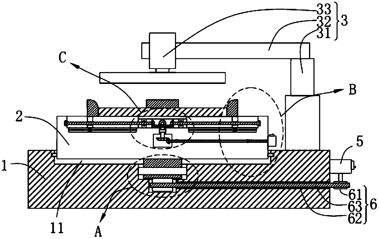
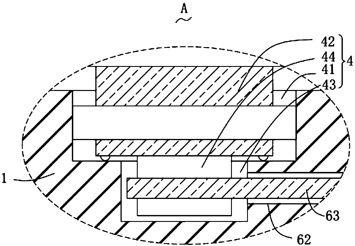
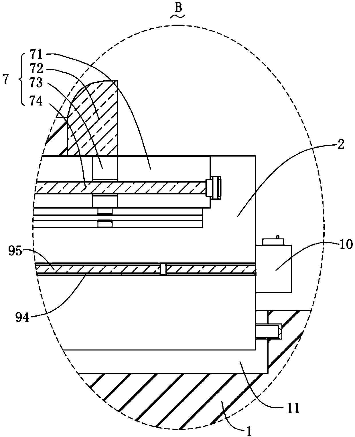
[0024] Please refer to figure 1 , figure 2 , image 3 , Figure 4 with Figure 5 ,among them, figure 1 It is a schematic front sectional view of a preferred embodiment of the dry film sticking device for thick copper PCB board production provided by the present invention; figure 2 for figure 1 The enlarged schematic diagram of part A shown; image 3 for figure 1 The enlarged schematic diagram of part B shown; Figure 4 for figure 1 The enlarged schematic diagram of part C shown; Figure 5 The assembly drawing of the first bevel gear and the second bevel gear in the dry film sticking device for thick copper PCB board production provided by the present invention. The dry film sticking device for thick copper PCB board production includes: a base 1; a turntable 2 which is rotatably mounted on the base 1; a film sticking structure 3, which is arranged on the top of the base 1


PUM


Abstract

The invention provides a dry film application device for the production of thick copper PCBs. The dry film application device for the production of thick copper PCBs comprises a base, a turntable, a film application structure, a rotating structure, a second motor and a first transmission structure. The turntable is rotationally installed on the base. The film application structure is arranged on the top of the base, and includes a first motor, a support rod and a push rod motor, wherein the first motor is fixedly installed on the top of the base. The rotating structure is arranged on the base,and includes a first groove, a first rotating shaft, a second groove and a first sprocket. The second motor is fixedly installed on one side of the base. The first transmission structure is arrangedon the base. The dry film application device for production of thick copper PCBs provided by the invention has the advantages of convenience of use, four-way clamping and limiting, avoidance of lateral displacement, easy rotation and adjustment of angle, and improvement of production efficiency.

Description


Claims


Application Information

Patent Timeline
Owner AOSHIKANG TECH CO LTD
Why Eureka
Try Eureka