Vertical cavity surface emitting laser of TO packaging

A technology of vertical cavity surface emission and lasers, which is applied in the direction of lasers, laser components, semiconductor lasers, etc., can solve the problems of low chip detection and monitoring efficiency, and achieve the effect of improving detector efficiency

Inactive Publication Date: 2008-07-30
INST OF SEMICONDUCTORS - CHINESE ACAD OF SCI
View PDF0 Cites 11 Cited by
  • Summary
  • Abstract
  • Description
  • Claims
  • Application Information

AI Technical Summary

Benefits of technology

This technology allows for efficient detection without being affected if there's any difference between two chips or planes. By placing both detectors closer together at one end, they emit more light towards each other instead of just facing upwards from them.

Problems solved by technology

In this patented technical solution for improving the design of vervacory surface emitter laser packages, there was introduced a new way to prevent unwanted sideways radiation when placing two chips together atop each other without interferring their signals. However, existing methods have limitations such as requiring high intensity light reflections due to poor coupling between the signal source and the photodetective element, causing decreased power output and lowered sensitivity.

Method used


Image

  • Vertical cavity surface emitting laser of TO packaging
  • Vertical cavity surface emitting laser of TO packaging
  • Vertical cavity surface emitting laser of TO packaging

Examples


Embodiment Construction

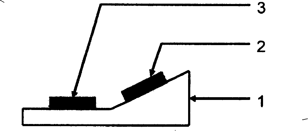
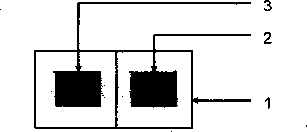
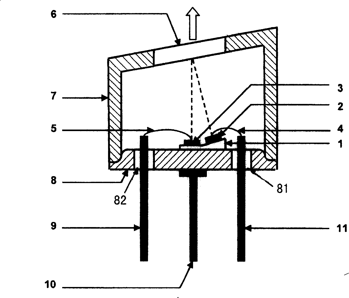
[0026] see figure 1 , figure 2 and image 3 ,Such as image 3 Shown, the vertical cavity surface emitting laser of a kind of TO package of the present invention, comprises:

[0027] A heat sink 1, the heat sink 1 is rectangular, and one end of the heat sink 1 is a slope; the heat sink 1 is made of oxygen-free high-conductivity copper or diamond or valve or silicon carbide or beryllium oxide or aluminum nitride etc. materials with high thermal conductivity and low expansion coefficient; the heat sink 1 prototype is obtained by wire cutting or etching; the upper and lower surfaces of the heat sink 1 are ground and polished; the upper and lower surfaces of the heat sink 1 are plated with gold; The heat sink 1 thus treated has good electrical and thermal conductivity;

[0028] A detector chip 2, the detector chip 2 is pasted on the inclined surface of one end of the heat sink 1 with solder; the effect of fixing the detector chip 2 on the heat sink 1 with solder is that the detec


PUM


Abstract

A vertical cavity surface emitting laser with TO package comprises a rectangular heat sink with an inclined surface on one end; a detector chip fixed on the inclined surface on one end of the heat sink; a laser chip fixed on the flat surface on one end of the heat sink; a round base with two via-holes thereon; two pins fixed in the two via-holes on the base; and a grounding pin fixed below the base, wherein the heat sink is fixed on the base; the detector chip is connected with the pins through wires; the laser chip is connected with the pins by wires; a cap covers the top of the base; and a lens is arranged on the cap.

Description


Claims


Application Information

Patent Timeline
Owner INST OF SEMICONDUCTORS - CHINESE ACAD OF SCI
Why Eureka
Try Eureka