Manufacturing method of metal interconnection structure
A technology of metal interconnection structure and manufacturing method, which is applied in semiconductor/solid-state device manufacturing, electrical components, circuits, etc., can solve the problems of difficult control of metal pattern shape and complicated process, and achieve easy control of metal pattern shape, simple process, The effect of doubling the graphics density
- Summary
- Abstract
- Description
- Claims
- Application Information
AI Technical Summary
Benefits of technology
Problems solved by technology
Method used
Image

Examples
Embodiment 1
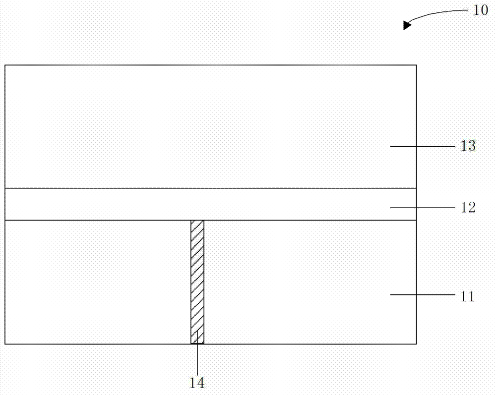
[0039] The fabrication method of the metal interconnection structure proposed by the present invention belongs to the back-end process (BEOL) in the field of semiconductors. Therefore, in this embodiment, the metal interconnection is formed on the conductive plug in the front layer of the metal interconnection structure. Taking the interconnection structure as an example, each step of the manufacturing method of the present invention is introduced in detail.
[0040] Step S11: providing a semiconductor substrate 10, the semiconductor substrate 10 has a front layer dielectric layer 11, an etching stop layer 12, and a dielectric sacrificial layer 13 in sequence from bottom to top.
[0041] see figure 1 As shown, a conductive plug 14 is formed in the front layer dielectric layer 11, and the conductive plug 14 is connected to the front layer metal pattern (not shown), so it is also called the front layer conductive plug 14; The base of the conductive plug 14 is the semiconductor su
Embodiment 2
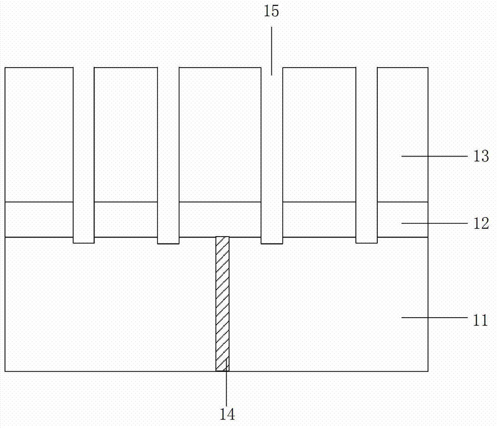
[0063] The metal interconnection structure and its method provided in the second embodiment are substantially the same as those in the first embodiment. The difference is that step S17 is also executed: if Figure 8 As shown, the sidewall 19 is removed to retain the filled metal 16 (that is, each set of metal patterns), and a low-K or ultra-low-K material 20 is filled between the metal 16 to form a low-K (2.0≤k≤4.0) or Metal interconnect structures with ultra-low K (k<2.0) dielectric layers. In this way, a low-K or ultra-low-K process double-patterning solution with smaller parasitic capacitance is provided, and the low-K or ultra-low-K material is not etched, so there are fewer defects.
Embodiment 3
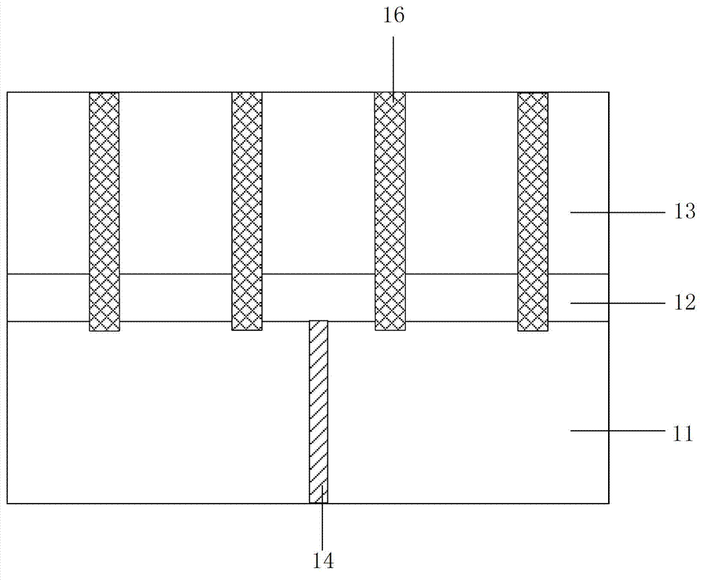
[0065] The metal interconnection structure and its method provided in the third embodiment are roughly the same as those in the first embodiment. The difference is that step S17' is also performed: as Figure 9 As shown, the spacer 19 is removed leaving the filled metal 16 (ie, sets of metal patterns) on which the capping layer 21 is deposited to form a metal interconnect structure with air gaps. Since the dielectric constant k of air is about 1.0, the parasitic capacitance can be further reduced compared with ordinary silicon dioxide (k>4.0), low-K (2.0≤k≤4.0) or ultra-low-K (k<2.0) materials.
[0066] In this embodiment, the capping layer 21 is an etching stop layer for the back-layer metal interconnection structure, and in other embodiments, other structures may also be provided as required.
[0067] In the present invention, each embodiment adopts a progressive writing method, focusing on the differences from the foregoing embodiments. For the same structures and manufacturi
PUM
 Abstract
Description
Claims
Application Information
 - R&D Engineer
- R&D Manager
- IP Professional
- Industry Leading Data Capabilities
- Powerful AI technology
- Patent DNA Extraction
Browse by: Latest US Patents, China's latest patents, Technical Efficacy Thesaurus, Application Domain, Technology Topic.
© 2024 PatSnap. All rights reserved.Legal|Privacy policy|Modern Slavery Act Transparency Statement|Sitemap