Buffer circuit and buffer chip
A buffer circuit and circuit technology, applied in the direction of logic circuit interface device, logic circuit connection/interface layout, etc., can solve the problems of complicated wiring, high cost, unfavorable large-scale expansion and use, etc., and achieve low cost, stable circuit and simple structure. Effect
- Summary
- Abstract
- Description
- Claims
- Application Information
AI Technical Summary
Problems solved by technology
Method used
Image


Examples
Embodiment 1
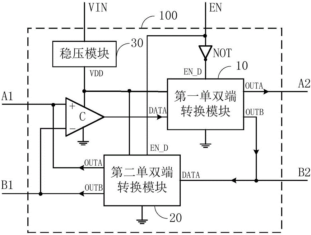
[0044] figure 1 It is a basic structural block diagram of the buffer circuit provided by Embodiment 1 of the present invention.
[0045] Such as figure 1 As shown, the buffer circuit 100 provided by this embodiment includes a first port A1, a second port B1, a third port A2, and a fourth port B2 for connecting to an external circuit. The circuit also includes an enable port EN, a differential amplifier C. NOT gate, first single-to-dual-end conversion module 10 and second single-to-dual-end conversion module 20 .
[0046] The non-inverting input terminal of the differential amplifier C is commonly connected with the first signal output terminal OUTA of the second single-to-double-ended conversion module 20 to form the first port A1, and the inverting input terminal of the differential amplifier C is connected to the The second signal output terminal OUTB of the second single-to-double-ended conversion module 20 is commonly connected to form the second port B1 , and the output te
Embodiment 2
[0066] figure 2 It is a basic structural block diagram of the buffer circuit provided by Embodiment 2 of the present invention.
[0067] Such as figure 2 As shown, the buffer circuit provided in this embodiment is a further extension based on the first embodiment.
[0068] In this embodiment, the buffer circuit 100 further includes a voltage stabilizing module 30 that is externally connected to a wide-voltage power supply VIN and outputs a constant voltage. The output terminal VDD of the voltage stabilizing module 30 is connected to the positive power supply terminal of the differential amplifier C, the The power supply terminal of the first single-to-double-terminal conversion module 10 and the power supply terminal of the second single-to-double-terminal conversion module 20 are connected in common.
[0069] In a specific application, the negative power terminal of the differential amplifier C, the ground terminal of the first single-to-dual-terminal conversion module 10 an
Embodiment 3
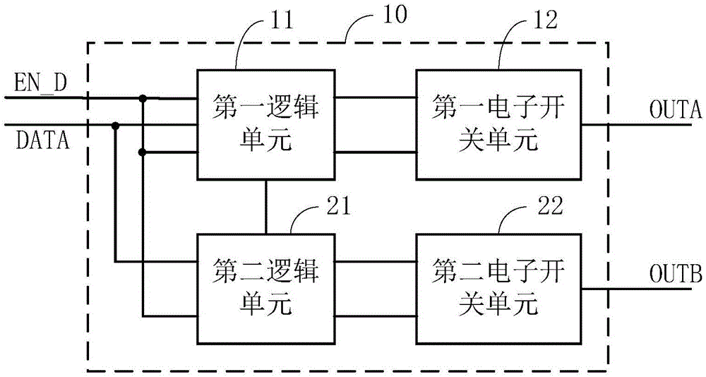
[0073] image 3 It is a basic structural block diagram of the first single-to-dual-end conversion module provided by Embodiment 3 of the present invention.
[0074] Such as image 3 As shown, this embodiment is in figure 1 or figure 2 A further refinement of the snubber circuit is shown.
[0075] In this embodiment, the first single-to-double conversion module 10 and the second single-to-double conversion module 20 have the same structure, and both include a first logic unit 11, a second logic unit 21, a first electronic switch unit 12 and a second Second, the electronic switch unit 22, the following takes the first single- and double-ended conversion module 10 as an example for specific description:
[0076] The first input terminal, the third input terminal of the first logic unit 11 and the third input terminal of the second logic unit 21 are commonly connected to form the enable terminal EN_D of the first single-to-double-ended conversion module 10;
[0077] The second
PUM
 Abstract
Description
Claims
Application Information
 - R&D Engineer
- R&D Manager
- IP Professional
- Industry Leading Data Capabilities
- Powerful AI technology
- Patent DNA Extraction
Browse by: Latest US Patents, China's latest patents, Technical Efficacy Thesaurus, Application Domain, Technology Topic.
© 2024 PatSnap. All rights reserved.Legal|Privacy policy|Modern Slavery Act Transparency Statement|Sitemap