Pixel structure and display device
A pixel structure and pixel technology, applied in the direction of static indicators, instruments, electrical components, etc., can solve the problems of mask processing difficulties, achieve the effect of solving the difficulty of opening processing and improving the yield
- Summary
- Abstract
- Description
- Claims
- Application Information
AI Technical Summary
Problems solved by technology
Method used
Image

Examples
Embodiment 1
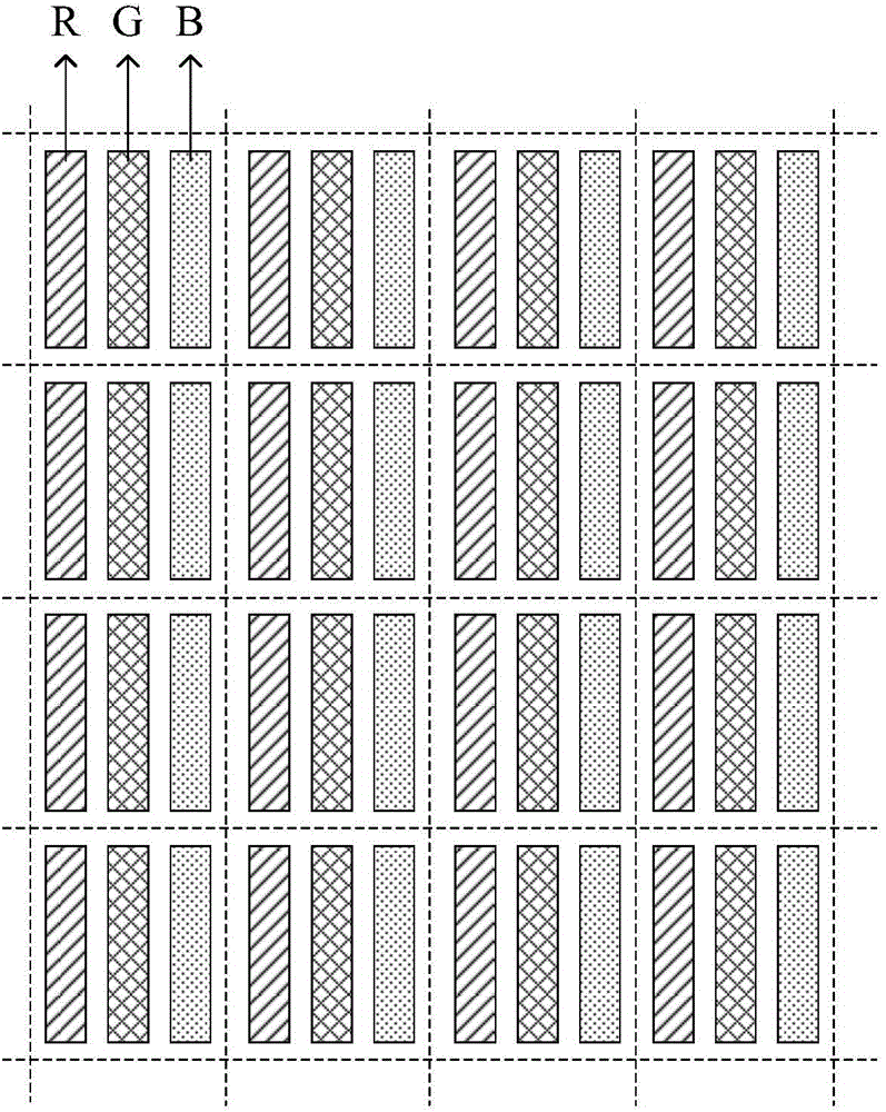
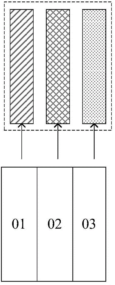
[0039] This embodiment provides a pixel structure, including a plurality of pixel units arranged in a matrix, and each pixel unit includes:
[0040] the first sub-pixel 100; and
[0041] At least two second sub-pixels 200 are juxtaposed and adjacent, and the organic materials of the at least two second sub-pixels 200 are connected to each other.
[0042]The second sub-pixel in the pixel unit corresponds to the electrode formed by etching the integrally formed organic material, that is, the step of forming the second sub-pixel includes two steps: the first step, etching to form one of the electrodes, and the second step, OLED organic materials are evaporated by FMM, and in the third step, the common electrodes of all OLEDs are evaporated. After the first step, the second sub-pixel is etched to form at least two independent electrodes, and then a red or blue organic material layer is formed on the substrate by evaporation using a mask plate. Although the organic material is integr
Embodiment approach 1
[0047] Embodiment 1: The color of the second sub-pixel in the sub-pixel unit is different from the color of the second sub-pixel in the adjacent sub-pixel units in the row direction, that is, the pixel units 10A are aligned in a row, as shown in the schematic diagram Figure 5 As shown, the pixel units in the row direction are distributed as red-green combination, blue-green combination, red-green combination, and blue-green combination, and the pixel units in the column direction are distributed as a red-green combination and a blue-green combination;
Embodiment approach 2
[0048] Embodiment 2: The color of the second sub-pixel in the sub-pixel unit is different from the color of the second sub-pixel in the adjacent sub-pixel units in the column direction, that is, the pixel units 10B are aligned in columns, as shown in the schematic diagram Figure 6 As shown, the pixel units in the column direction are distributed as red-green combination, blue-green combination, red-green combination, and blue-green combination, and the pixel units in the row direction are distributed as a red-green combination and a blue-green combination;
PUM
 Abstract
Description
Claims
Application Information
 - R&D Engineer
- R&D Manager
- IP Professional
- Industry Leading Data Capabilities
- Powerful AI technology
- Patent DNA Extraction
Browse by: Latest US Patents, China's latest patents, Technical Efficacy Thesaurus, Application Domain, Technology Topic.
© 2024 PatSnap. All rights reserved.Legal|Privacy policy|Modern Slavery Act Transparency Statement|Sitemap