Liquid crystal display panel
A liquid crystal display panel and non-display area technology, applied in nonlinear optics, instruments, optics, etc., can solve the problems of immeasurable cost loss, insufficient light transmittance of edge circuits, and inability to realize production line monitoring and inspection functions, etc. Achieve the effect of improving the light transmittance of the edge
- Summary
- Abstract
- Description
- Claims
- Application Information
AI Technical Summary
Benefits of technology
Problems solved by technology
Method used
Image

Examples
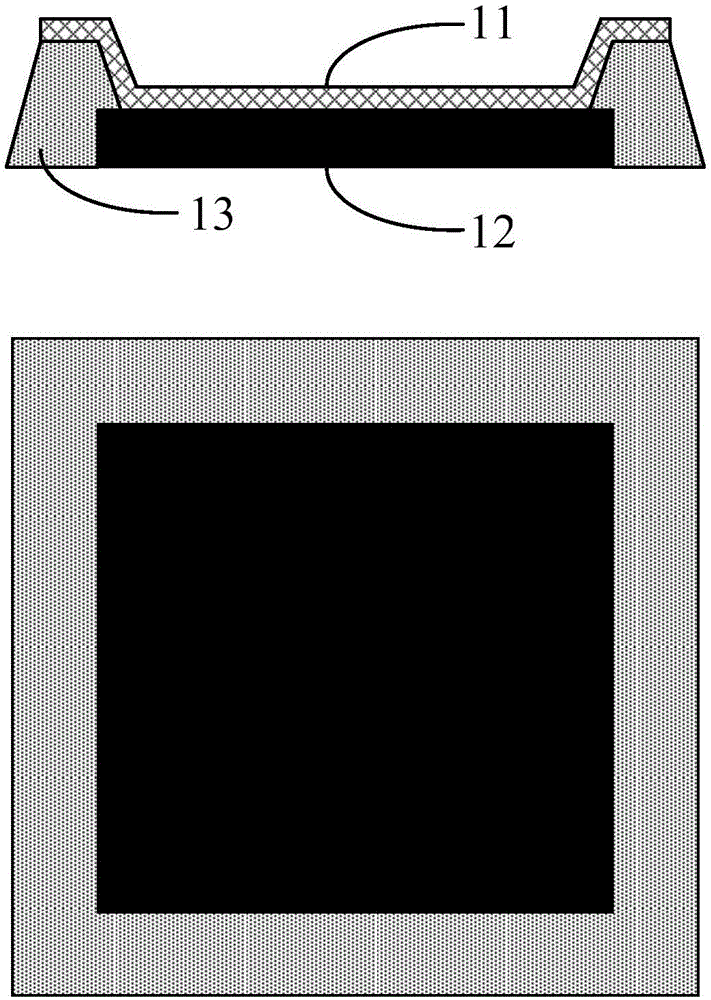
no. 1 example
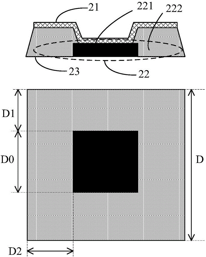
[0029] figure 2 is a cross-sectional view and a top view of the test pad structure according to the first embodiment, such as figure 2 As shown, 21 is a surface contact layer, 22 is a signal transmission layer, and 23 is a protective layer. In this embodiment, the signal transmission layer 22 is divided into a non-hollow area 221 and a hollow area 222 . The non-hollowed-out area 221 is located in the central area of the entire test pad, and the hollowed-out area 222 is arranged around the non-hollowed-out area 221 .
[0030] Only one via hole is provided on the protection layer 23 , and the via hole corresponds to the central area of the test pad and is provided directly above the non-hollowed-out area 221 . The signal transmission layer 21 communicates with the non-hollowed-out area 221 through via holes to realize the transmission of test signals.
[0031] In order to improve the light transmittance of the frame area, in this embodiment, it is necessary to ensure that
no. 2 example
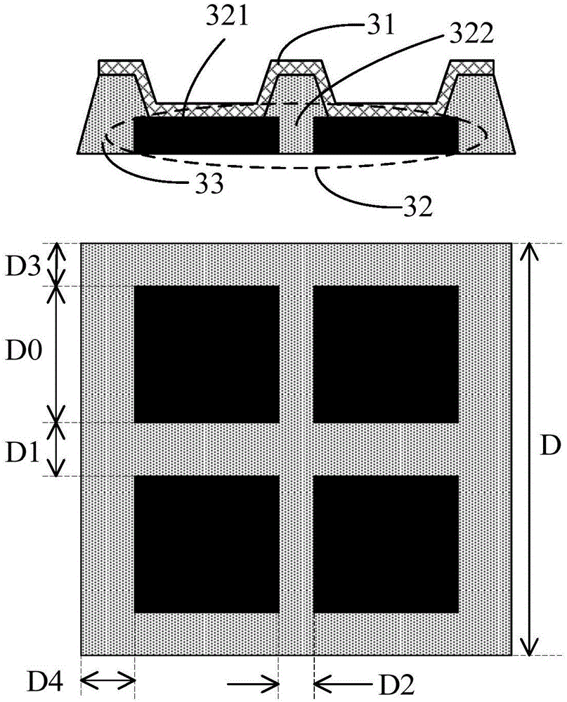
[0037] image 3 is a cross-sectional view and a top view of the test pad structure according to the second embodiment, such as image 3 As shown, 31 is a surface contact layer, 32 is a signal transmission layer, and 33 is a protective layer. In this embodiment, the signal transmission layer 32 is divided into a non-hollow area 321 and a hollow area 322 . The non-hollowed out area 321 is in the form of a plurality of discrete blocks scattered throughout the area of the test pad, and the hollowed out area 322 is formed in the area between the individual blocks.
[0038] Via holes equal to the number of blocks are provided on the protective layer 33 , and each via hole is provided corresponding to each block. combine image 3 It can be seen from the cross-sectional view and top view in the figure that each via hole is respectively arranged directly above each block.
[0039] Preferably, in order to balance the requirements on the light transmittance of the area and the increas
no. 3 example
[0047] Figure 4 is a cross-sectional view and a top view of the test pad structure according to the third embodiment, such as Figure 4 As shown, 41 is a surface contact layer, 42 is a signal transmission layer, and 43 is a protective layer. In this embodiment, the signal transmission layer 42 is divided into a non-hollow area 421 and a hollow area 422 . Specifically, the signal transmission layer 42 is a grid-like structure formed by metal, on which the non-hollowed-out area 421 and the hollowed-out area 422 are spaced apart from each other.
[0048] A plurality of via holes are provided on the protection layer 33 , and the positions of the via holes correspond to the non-hollowed-out parts of the grid structure.
[0049] In this embodiment, there is no limitation on the number of via holes to be opened. In theory, as many via holes as possible can be opened under the premise of balancing processing difficulty and processing cost.
[0050] Similarly, in this embodiment, the
PUM
 Abstract
Description
Claims
Application Information
 - R&D Engineer
- R&D Manager
- IP Professional
- Industry Leading Data Capabilities
- Powerful AI technology
- Patent DNA Extraction
Browse by: Latest US Patents, China's latest patents, Technical Efficacy Thesaurus, Application Domain, Technology Topic.
© 2024 PatSnap. All rights reserved.Legal|Privacy policy|Modern Slavery Act Transparency Statement|Sitemap