Mercury cadmium telluride avalanche diode detector capable of modulating surface energy band

An avalanche diode, mercury cadmium telluride technology, applied in semiconductor devices, electrical components, circuits, etc., can solve problems such as photodiode thermoelectric breakdown, and achieve the effect of suppressing surface leakage current

Pending Publication Date: 2018-11-13
SHANGHAI INST OF TECHNICAL PHYSICS - CHINESE ACAD OF SCI
View PDF0 Cites 4 Cited by
  • Summary
  • Abstract
  • Description
  • Claims
  • Application Information

AI Technical Summary

Benefits of technology

This technology solves problems with traditional devices used for detecting signals during operation at high voltages caused by backward biased electrons from an n-type semiconductor material called Cadmium Tellurate (CdTe). However, this issue can lead to thermal damage or even failure if too much electricity flows through certain regions near CdTe's electrodes. To address these issues, researchers have developed techniques such as modifying the crystal structure of quantum well layers within the CdTjunction area to reduce surface electrical conductivity and prevent excessive heat generation due to increased temperature.

Problems solved by technology

The technical problem addressed by this patented method described in the patented text relates to improving the performance and efficiency of semiconductor devices that use quantum cascade laser absorption spectroscopy (QCLS) techniques like gamma ray cameras. These devices require specific types of crystals called Cadmocalcene Tellurite Indicta Cd_xcd TAPHARDS), but traditional methods cannot provide these materials without sacrificial layers. To overcome this issue, researchers proposed new ways to improve their ability to detect light waves while minimizing unwanted background radiation levels.

Method used


Image

  • Mercury cadmium telluride avalanche diode detector capable of modulating surface energy band
  • Mercury cadmium telluride avalanche diode detector capable of modulating surface energy band
  • Mercury cadmium telluride avalanche diode detector capable of modulating surface energy band

Examples


Embodiment 1

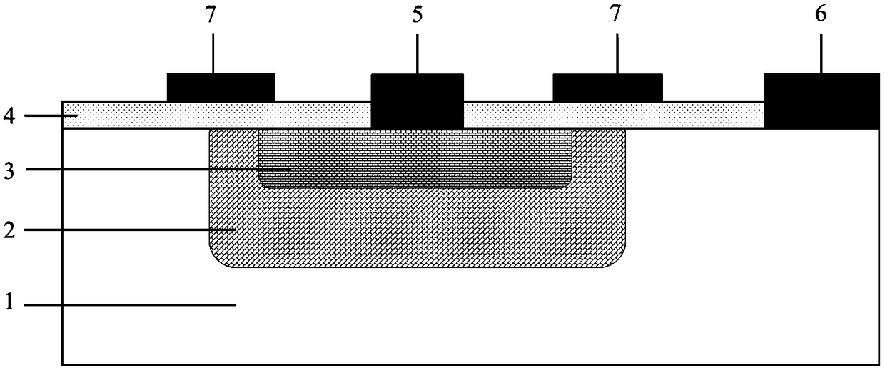
[0014] 1) Form n on p-type HgCdTe by conventional doping + -n - -p structure, HgCdTe p region concentration is 8×10 15 cm -3 , n - Zone concentration is 1 x 10 15 cm -3 , longitudinal n + n under the area - Zone thickness is 3 μm, n + Zone concentration is 1 x 10 17 cm -3 , with a thickness of 1 μm;

[0015] 2) First grow a 100nm cadmium telluride passivation layer on the surface of mercury cadmium telluride;

[0016] 3) Corroding the passivation layer with a cadmium telluride etching solution to open passivation holes in the pn junction photosensitive element area and common electrode passivation holes in the p area;

[0017] 4) 20 nm of tin is grown on the passivation hole and the passivation layer of the pn junction depletion region, and 60 nm of gold is grown.

Embodiment 2

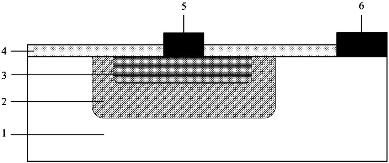
[0019] 1) Form n on p-type HgCdTe by conventional doping + -n - -p structure, HgCdTe p region concentration is 8×10 15 cm -3 , n - Zone concentration is 1 x 10 15 cm -3 , longitudinal n + n under the area - Zone thickness is 3 μm, n + Zone concentration is 1 x 10 17 cm -3 , with a thickness of 1 μm;

[0020] 2) On the surface of mercury cadmium telluride, a 150nm cadmium telluride passivation layer is first grown, and then 100nm of zinc sulfide is grown;

[0021] 3) Corroding the zinc sulfide with hydrochloric acid, corroding the passivation layer with cadmium telluride corrosion solution, and opening the passivation hole in the pn junction photosensitive element area and the common electrode passivation hole in the p area;

[0022] 4) 30 nm of tin is grown on the passivation hole and the passivation layer of the pn junction depletion region, and 100 nm of gold is grown.

Embodiment 3

[0024] 1) Form n on p-type HgCdTe by conventional doping + -n - -p structure, HgCdTe p region concentration is 8×10 15 cm -3 , n - Zone concentration is 1 x 10 15 cm -3 , longitudinal n + n under the area - Zone thickness is 3 μm, n + Zone concentration is 1 x 10 17 cm -3 , with a thickness of 1 μm;

[0025] 2) On the surface of mercury cadmium telluride, a 200nm cadmium telluride passivation layer is first grown, and then 200nm of zinc sulfide is grown;

[0026] 3) Corroding the zinc sulfide with hydrochloric acid, corroding the passivation layer with cadmium telluride corrosion solution, and opening the passivation hole in the pn junction photosensitive element area and the common electrode passivation hole in the p area;

[0027] 4) 40 nm of tin is grown on the passivation hole and the passivation layer of the pn junction depletion region, and 120 nm of gold is grown.


PUM

PropertyMeasurementUnit
Thicknessaaaaaaaaaa
Thicknessaaaaaaaaaa
Thicknessaaaaaaaaaa

Abstract

The invention discloses a mercury cadmium telluride avalanche diode detector capable of modulating a surface energy band. By adding an electrode above a passivation layer of a pn junction depletion region, the pn junction energy band at the interface between the passivation layer and the mercury cadmium telluride can be modulated, and the pn junction at the interface between the passivation layerand the mercury cadmium telluride tends to be flat, thereby suppressing surface generation-recombination, surface tunneling, and surface leakage currents. The detector has the advantages that the surface energy band of the pn junction region can be modulated to be flat, and the surface leakage current is suppressed to enable the diode to work in the Geiger mode under the reverse large bias voltage, which is advantageous for solving the problem that the mercury cadmium telluride avalanche diode device of the conventional structure may have large leakage current at the surface when the reverse bias voltage is greater than the avalanche breakdown voltage, causes the photodiode to undergo thermal-electric breakdown, and limits signal detection in a linear mode.

Description


Claims


Application Information

Patent Timeline
Owner SHANGHAI INST OF TECHNICAL PHYSICS - CHINESE ACAD OF SCI
Why Eureka
Try Eureka