Optical waveguide and method for manufacturing the same
- Summary
- Abstract
- Description
- Claims
- Application Information
AI Technical Summary
Problems solved by technology
Method used
Image

Examples
first exemplary embodiment
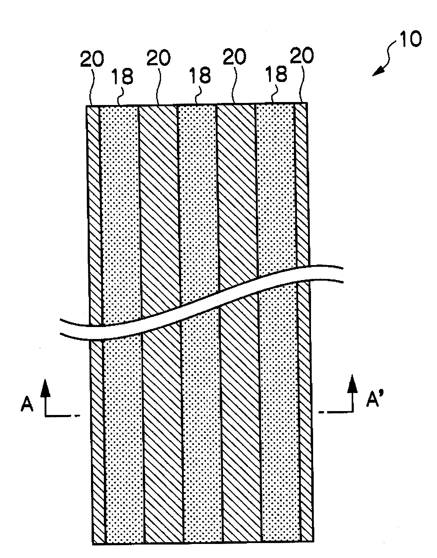
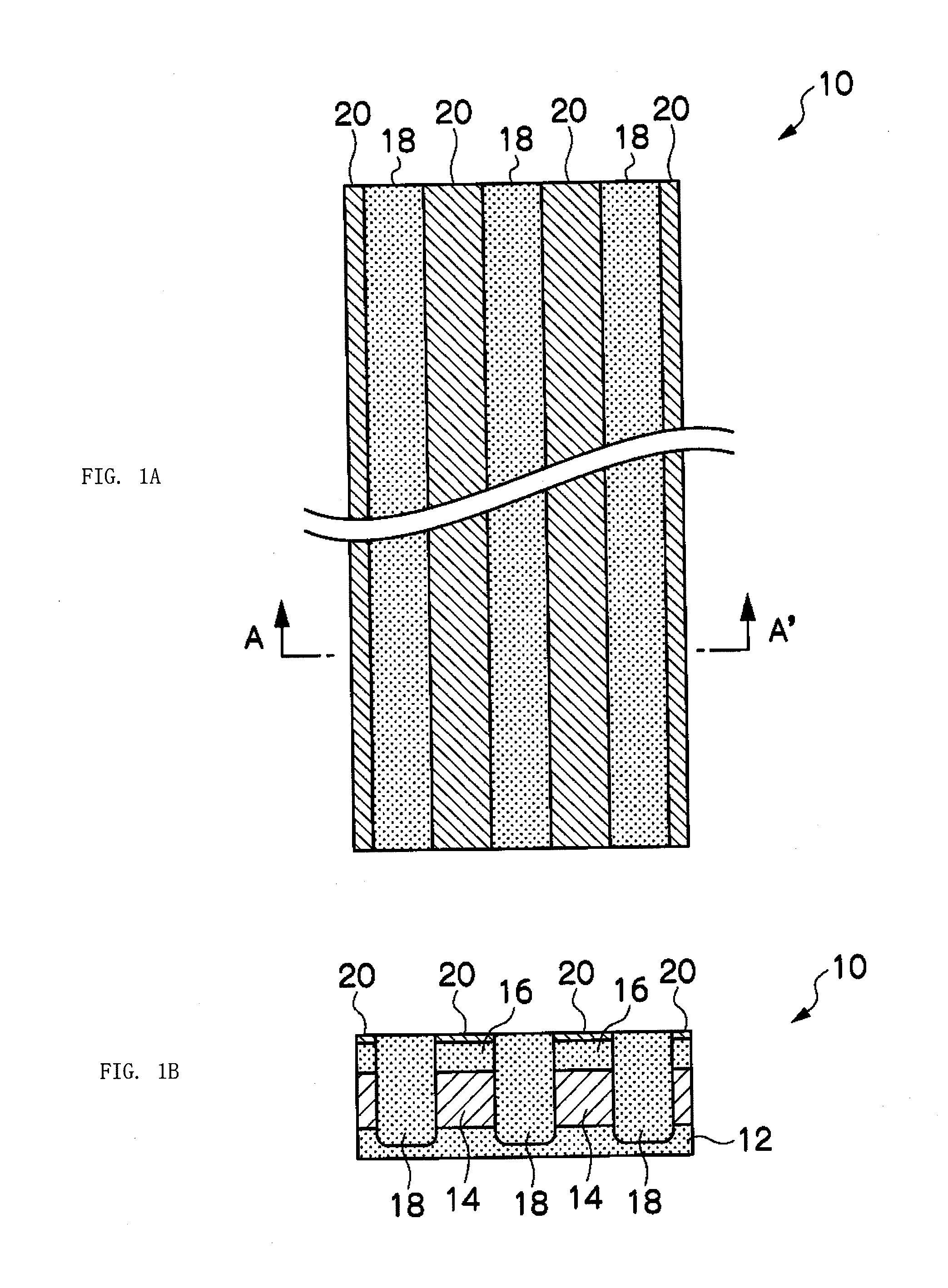
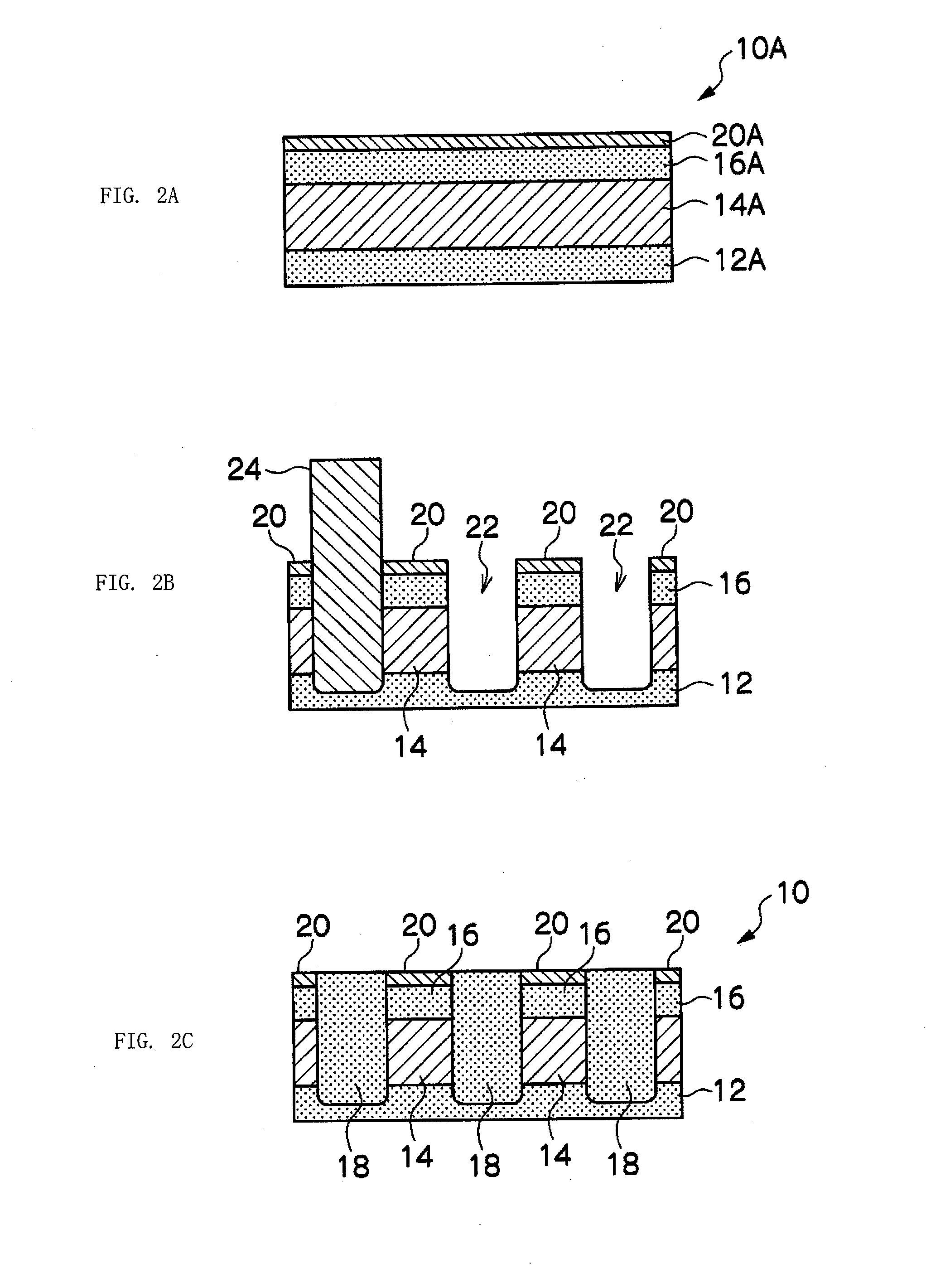
[0024]FIGS. 1A and 1B schematically show the configuration of the optical waveguide according to the first exemplary embodiment of the invention. The optical waveguide 10 is a planar optical waveguide. Aplurality of cores 14 are embedded in a cladding (lower cladding portion 12, upper cladding portions 16 and embedded cladding portions 18) in parallel to each other on a plane parallel to the principal surfaces of the optical waveguide 10. Colored layers 20 are provided on the portions that substantially overlap the respective cores 14 when viewed from a direction substantially perpendicular to the principal surfaces of the optical waveguide 10. Here, among the surfaces of the optical waveguide 10, the principal surface refers to a surface substantially perpendicular to the direction of lamination (the thickness direction of the optical waveguide 10) of the core 14 and cladding portions (lower cladding portion 12 and upper cladding portion 16) that are laminated so as to sandwich the co
second exemplary embodiment
[0047]FIG. 3A and FIG. 3B schematically show the configuration of an optical waveguide according to a second exemplary embodiment. As shown in FIG. 3B, the optical waveguide 30 has two colored layers (a first colored layer 20a and a second colored layer 20b) having different colors from each other at one principal surface side (between the core 14 and one of the principal surfaces of the optical waveguide 30) of the optical waveguide 40 with respect to the core 14. The colored layer 20a is layered on a first upper cladding portion 16a, and the colored layer 20b is layered on a second upper cladding portion 16b. The colored layers 20a and 20b are not in contact with the core 14. In this exemplary embodiment, two cut grooves 22a and 22b are formed by cutting away portions from the second color layer 20b to a part of the lower cladding portion 12. Each of the grooves 22a and 22b is filled with an embedded cladding portion 18. Meanwhile, another cut groove 22c is formed by cutting a portio
third exemplary embodiment
[0049]FIG. 4A and FIG. 4B schematically show the configuration of an optical waveguide according to a third exemplary embodiment. As shown in FIG. 4B, a first colored layer 20a and a second colored layer 20b having different colors from each other are provided on one principal surface side of the optical waveguide with respect to cores 14a and 14b (between the cores 14a, 14b and one of the principal surfaces of the optical waveguide 40) without contacting the cores 14a and 14b. In this optical waveguide 40, the two core portions 14a and 14b are formed by three cut grooves 22a, 22b and 22c formed by cutting portions from the second colored layer 22b to a part of a lower cladding portion 12. Further, an embedded cladding portion 18 is embedded in a portion formed by removing the second colored layer 20b corresponding to the core portion 14b.
[0050]Thus, as shown in FIG. 4A, when viewed from the direction substantially perpendicular to the principal surface of the optical waveguide 40, ei
PUM
| Property | Measurement | Unit |
|---|---|---|
| Thickness | aaaaa | aaaaa |
| Color | aaaaa | aaaaa |
| Refractive index | aaaaa | aaaaa |
Abstract
Description
Claims
Application Information
 - R&D Engineer
- R&D Manager
- IP Professional
- Industry Leading Data Capabilities
- Powerful AI technology
- Patent DNA Extraction
Browse by: Latest US Patents, China's latest patents, Technical Efficacy Thesaurus, Application Domain, Technology Topic.
© 2024 PatSnap. All rights reserved.Legal|Privacy policy|Modern Slavery Act Transparency Statement|Sitemap