Optical modulation method and system
- Summary
- Abstract
- Description
- Claims
- Application Information
AI Technical Summary
Benefits of technology
Problems solved by technology
Method used
Image

Examples
Example
[0024]FIG. 1 is a flow chart of a method according to a first embodiment of the present invention, which includes the following steps:
[0025]Step 11: Load a first dither signal on an amplitude of an input data signal.
[0026]For example, load the first dither signal on the amplitude of the data signal by using a multiplier.
[0027]Step 12: Load a second dither signal on a bias voltage.
[0028]For example, load the second dither signal on the bias voltage by using an adder.
[0029]The first dither signal and the second dither signal are signals of the same frequency and the same phase, and a ratio of amplitudes of the signals is determined according to a tracking error, so that a feedback signal obtained according to the modulation signal is locked to a required bias point.
[0030]The first dither signal and the second dither signal may be obtained by performing different types of amplification processing on a source dither signal. For example, this embodiment may also include: obtaining a source
Example
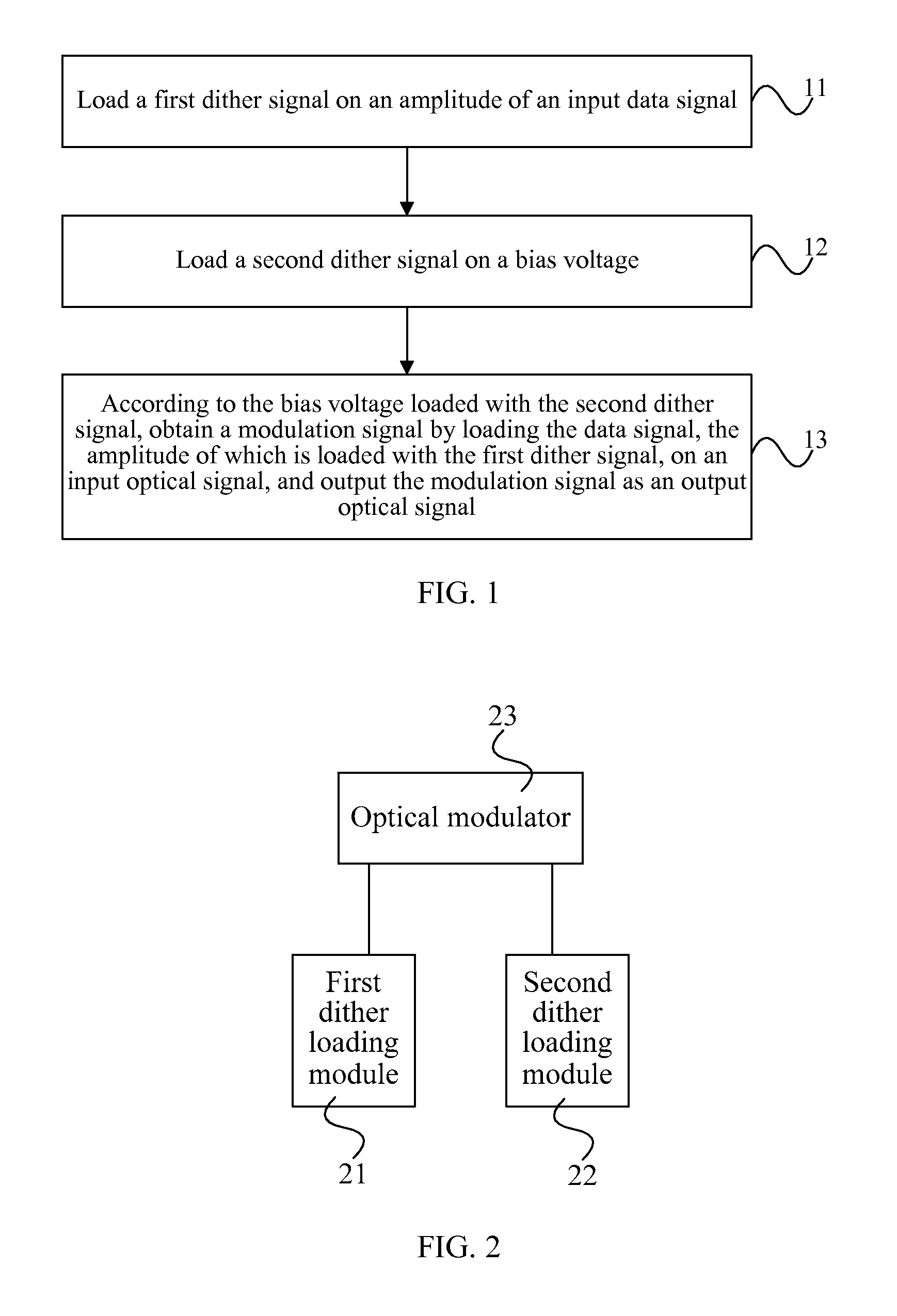
[0036]FIG. 2 is a schematic structural diagram of a system according to a second embodiment of the present invention, which includes: a first dither loading module 21, a second dither loading module 22, and an optical modulator 23. The first dither loading module 21 is configured to load a first dither signal on an amplitude of an input data signal. The second dither loading module 22 is configured to load a second dither signal on a bias voltage. The optical modulator 23 is configured to, according to the bias voltage loaded with the second dither signal, obtain a modulation signal by loading the data signal, the amplitude of which is loaded with the first dither signal, on an input optical signal, and output the modulation signal as an output optical signal. The first dither signal and the second dither signal are signals of the same frequency and the same phase, and a ratio of amplitudes of the signals is determined according to a tracking error, so that a feedback signal obtained a
Example
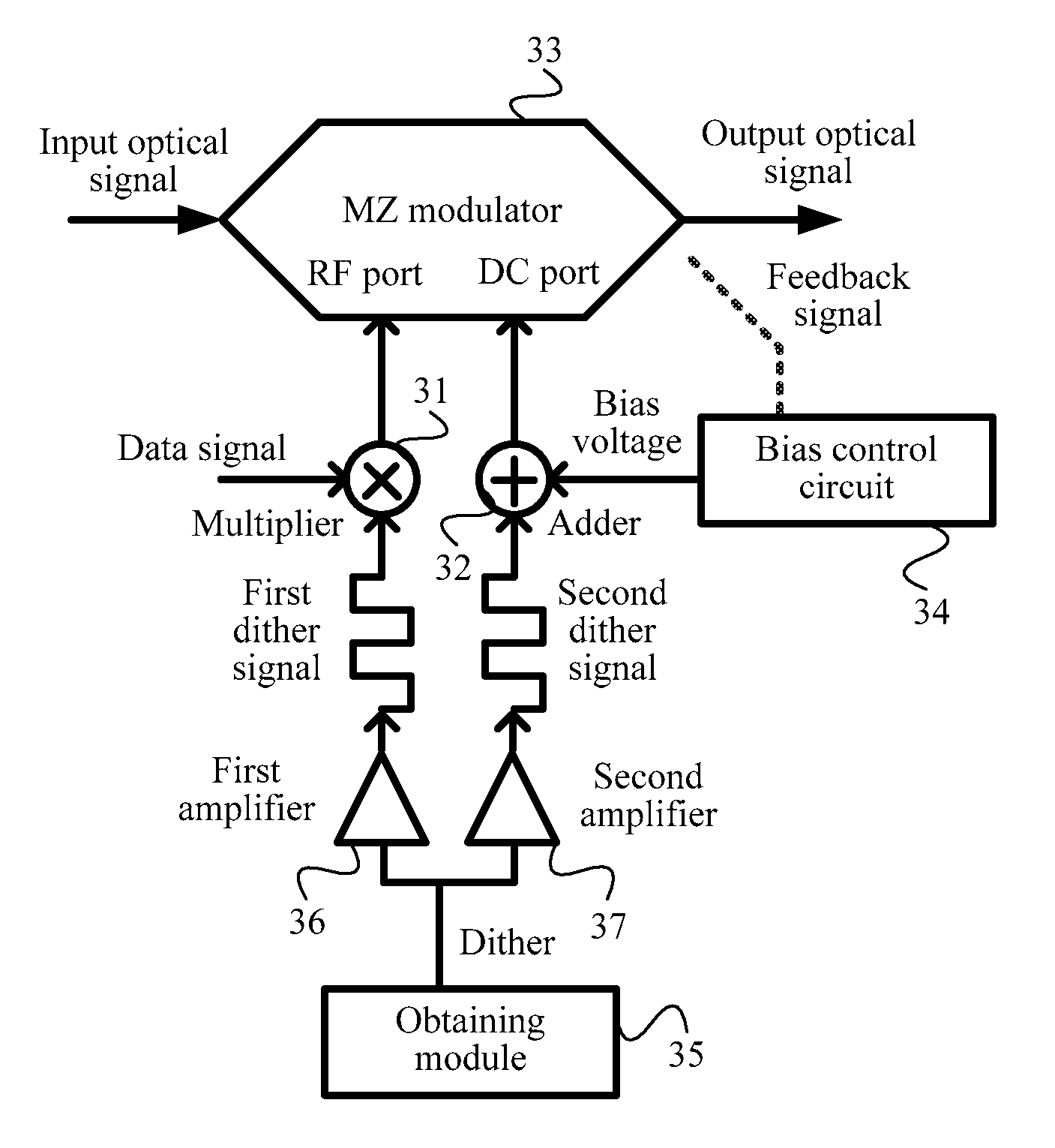
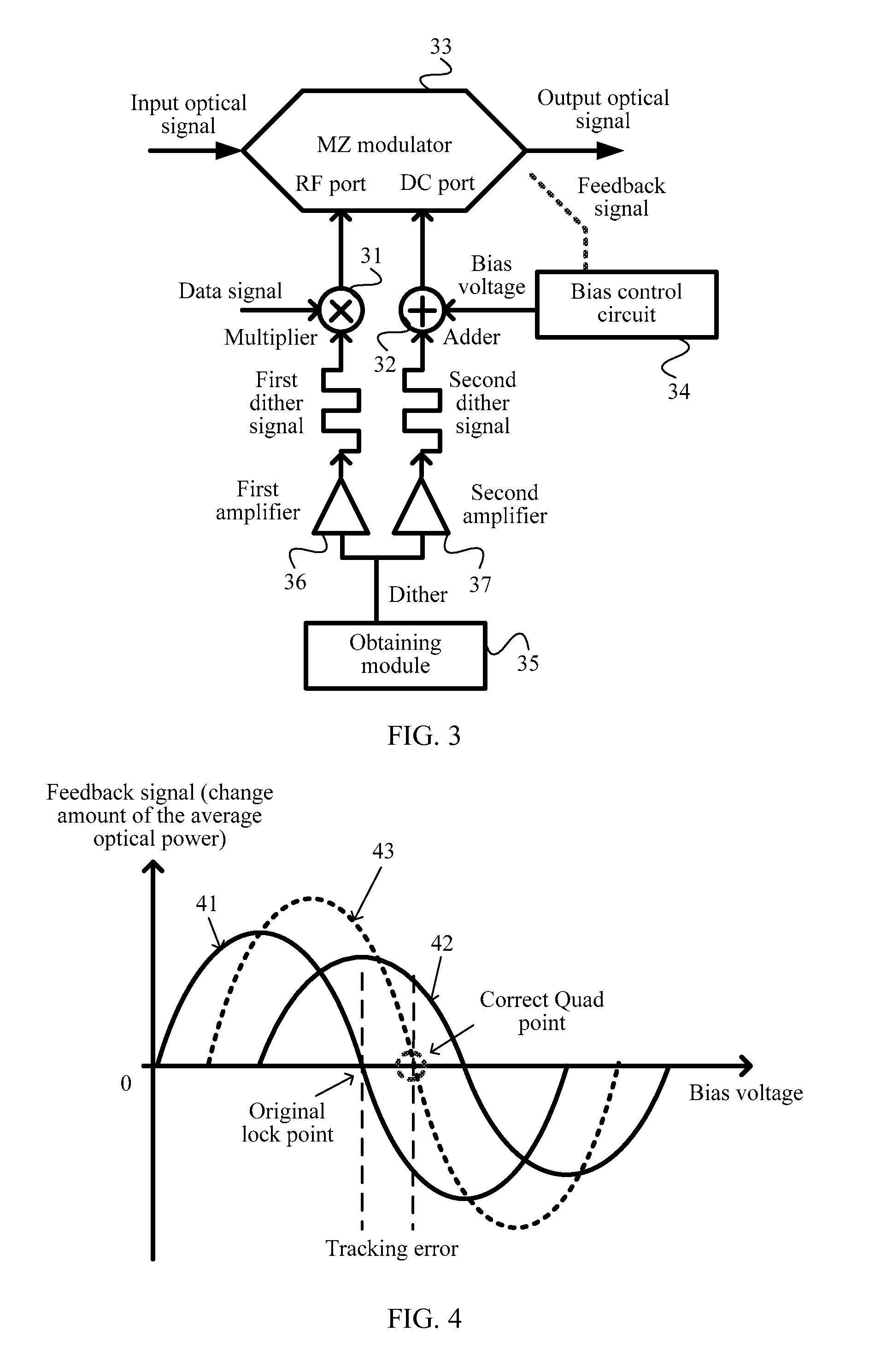
[0037]FIG. 3 is a schematic structural diagram of a system according to a third embodiment of the present invention. In this embodiment, it is taken as an example that an optical modulator is an MZ modulator, a first dither loading module is a multiplier, a second dither loading module is an adder, and a first dither signal and a second dither signal are obtained after performing different types of amplification on a source dither signal respectively.
[0038]This embodiment includes: a multiplier 31, an adder 32, an MZ modulator 33, a bias voltage controller (Bias control circuit) 34, a first amplifier 36, a second amplifier 37, and an obtaining module 35.
[0039]The obtaining module 35 is configured to obtain the source dither signal. The first amplifier 36 is configured to obtain the first dither signal after performing amplification processing on the source dither signal. The multiplier 31 is configured to load the first dither signal on an amplitude of an input data signal. The second
PUM
 Abstract
Description
Claims
Application Information
 - R&D Engineer
- R&D Manager
- IP Professional
- Industry Leading Data Capabilities
- Powerful AI technology
- Patent DNA Extraction
Browse by: Latest US Patents, China's latest patents, Technical Efficacy Thesaurus, Application Domain, Technology Topic.
© 2024 PatSnap. All rights reserved.Legal|Privacy policy|Modern Slavery Act Transparency Statement|Sitemap