Adaptive interface for coupling FPGA modules
a module and interface technology, applied in the direction of logic circuit coupling/interface arrangement, pulse technique, instruments, etc., can solve the problems of high cost, inability to adapt to the i/o wiring of module fpga circuits or model fpga circuits in prototyping systems, etc., to achieve low cost, low latency, and high data rate
- Summary
- Abstract
- Description
- Claims
- Application Information
AI Technical Summary
Benefits of technology
Problems solved by technology
Method used
Image

Examples
Embodiment Construction
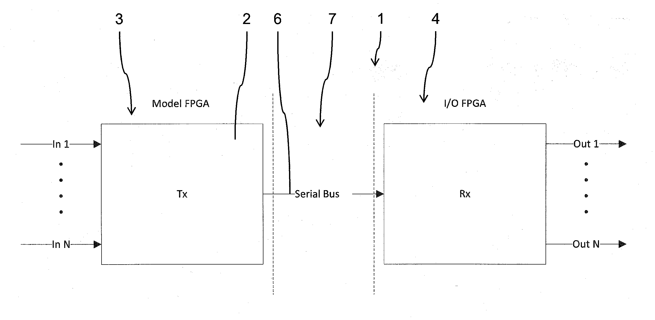
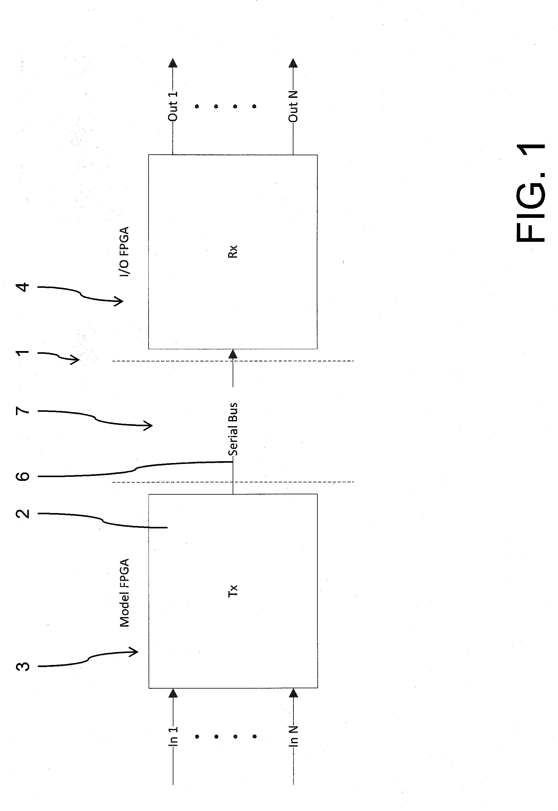
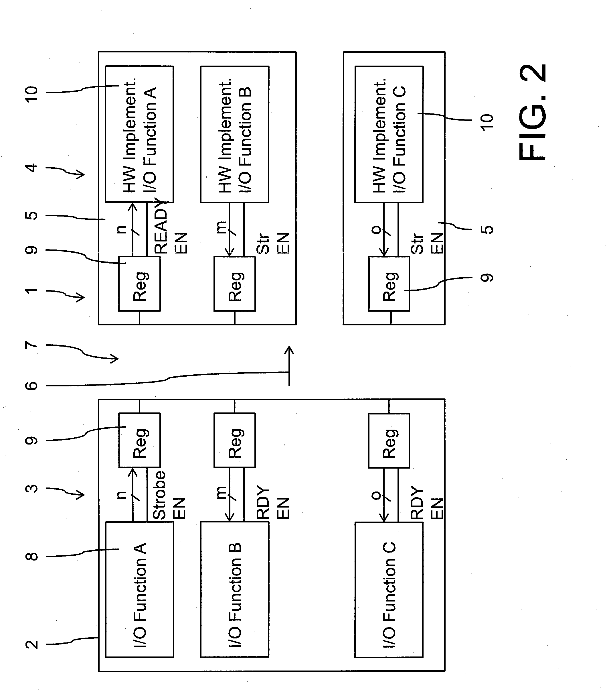
[0049]FIG. 1 shows an FPGA control system 1 according to a preferred embodiment. FPGA control system 1 comprises an FPGA 2 as sender side 3 and a receiver side 4. Receiver side 4 in this exemplary embodiment comprises two I / O modules 5, as is shown in the detail in FIG. 2.
[0050]A serial interface 6 is formed between sender side 3 and receiver side 4. Serial interface 6 is the basis for an adaptive interface 7, which is implemented between FPGA 2 and I / O modules 5 and uses serial interface 6 as the transmission medium. Serial interface 6 is realized as an LVDS interface with a block size of 8 bits for the transmission of data
[0051]A plurality of FPGA applications 8, each of which is connected via register 9 to adaptive interface 7, is implemented in FPGA 2. On receiver side 4 a plurality of hardware implementations 10 is formed in I / O modules 5, which are also connected via register 9 to adaptive interface 7.
[0052]Further, a method for implementing adaptive interface 7 between FPG
PUM
 Abstract
Description
Claims
Application Information
 - R&D Engineer
- R&D Manager
- IP Professional
- Industry Leading Data Capabilities
- Powerful AI technology
- Patent DNA Extraction
Browse by: Latest US Patents, China's latest patents, Technical Efficacy Thesaurus, Application Domain, Technology Topic.
© 2024 PatSnap. All rights reserved.Legal|Privacy policy|Modern Slavery Act Transparency Statement|Sitemap