Optical device, laser beam source, laser apparatus and method of producing optical device
- Summary
- Abstract
- Description
- Claims
- Application Information
AI Technical Summary
Benefits of technology
Problems solved by technology
Method used
Image

Examples
example 1
[0143]Referring to FIG. 7, Example 1 of the present invention will be described.
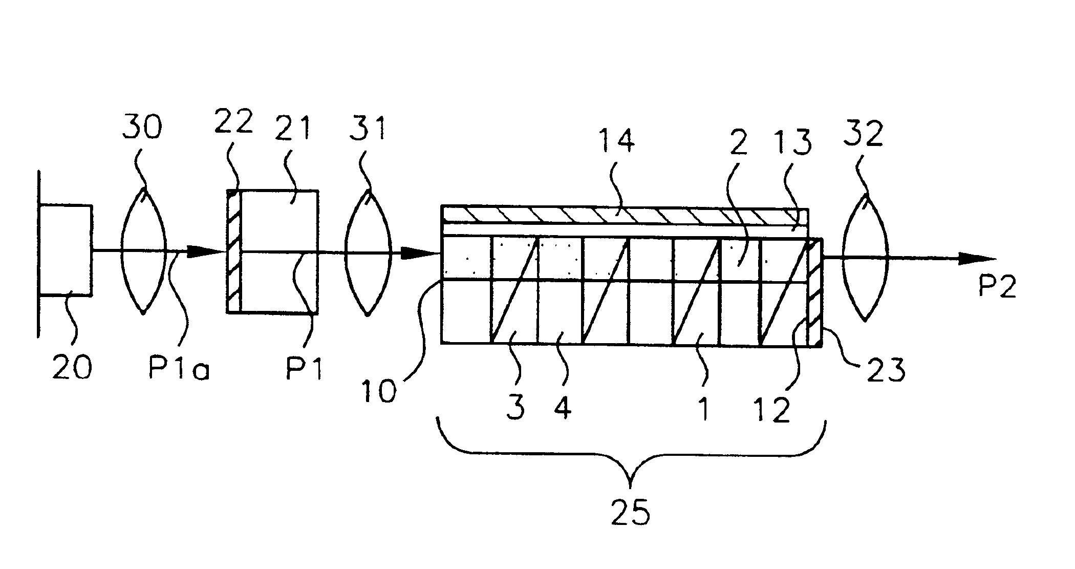
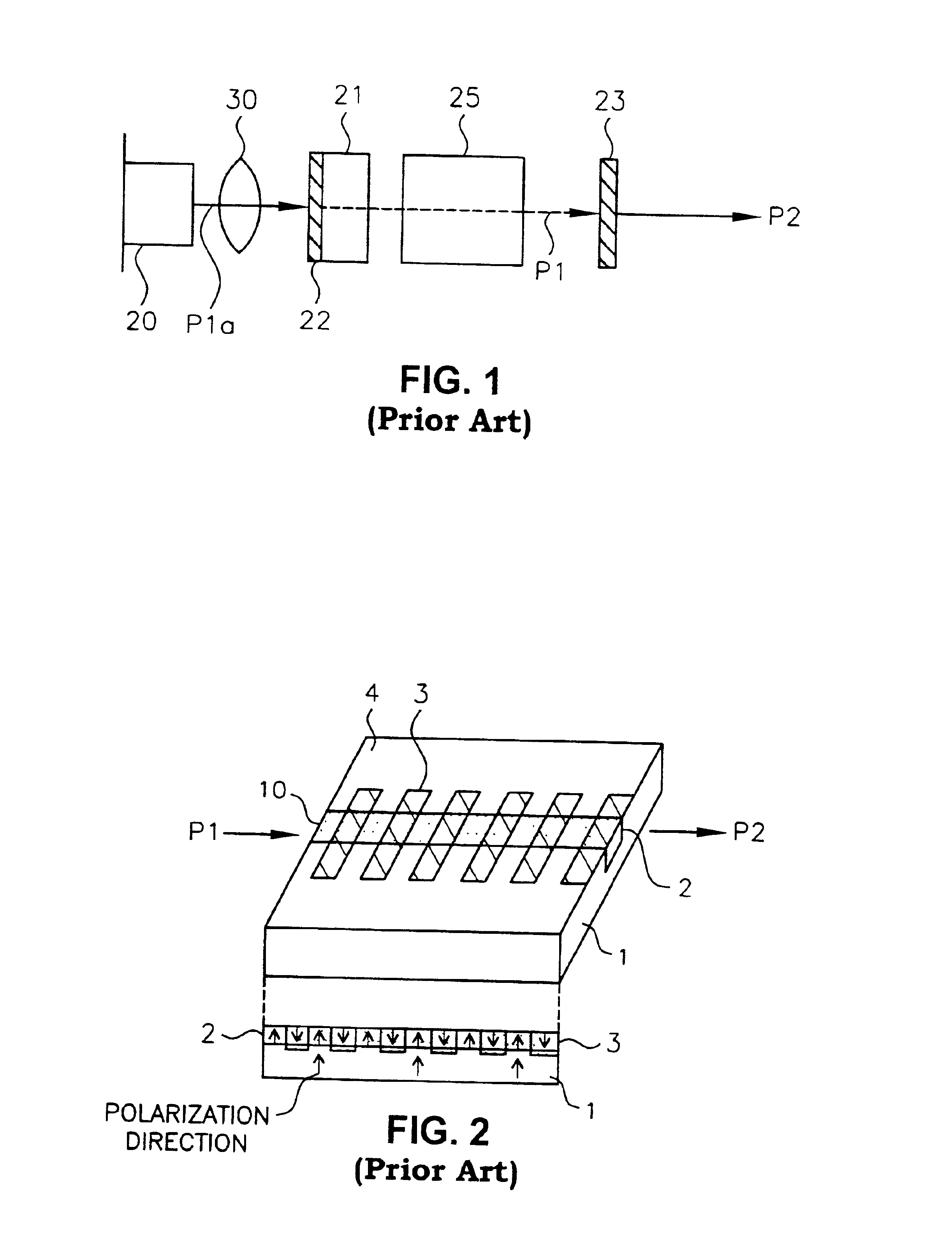
[0144]In an optical wavelength conversion element of the present example, an optical waveguide of a stable proton exchange layer is formed in an LiTaO3 substrate 1, and a plurality of domain inverted layers 3 are periodically arranged along the optical waveguide. By making a fundamental wave P1 incident upon an input end of the optical waveguide, a harmonic wave P2 is emitted from an output end thereof. The length of the optical wavelength conversion element (length of the optical waveguide) is 9 mm in the present example. Moreover, in order to allow for operation at a wavelength of 850 nm, the length of a pitch of the domain inverted layers 3 is set to 3.7 μm.
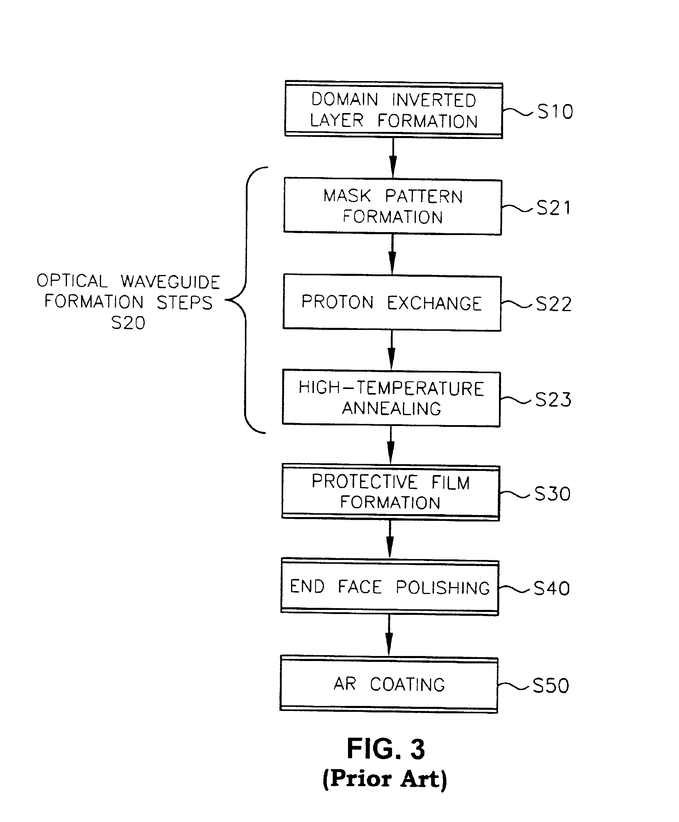
[0145]Hereinafter, referring to FIGS. 8A to 8E, a production method of the optical wavelength conversion element will be described.
[0146]First, as shown in FIG. 8A, a Ta film is deposited so as to cover the principal surface of the LiTaO3 substrate 1,
example 2
[0160]Next, Example 2 of the present invention will be described.
[0161]First, a Ta film is deposited so as to cover the principal surface of the LiTaO3 substrate, after which ordinary photolithography and dry etching techniques are used to pattern the Ta film (thickness: about 200 to 300 nm) into a striped pattern, thereby forming the Ta mask. The Ta mask used in the present example has a pattern where strips each 1.2 μm wide and 10 mm long are arranged so as to be equally spaced apart from one another, and the arrangement pitch of the strips is 3.6 μm. A proton exchange process is performed for the LiTaO3 substrate 1 whose principal surface is covered by the Ta mask. The proton exchange process is performed by immersing the surface of the substrate for 20 minutes in a pyrophosphoric acid heated to 260° C. Thus, 0.5μm thick proton exchange layers are formed in portions of the LiTaO3 substrate 1 which are not covered by the Ta mask. Then, the Ta mask is removed by etching for 2 minutes
example 3
[0169]Next, as Example 3 of the present invention, a case of using an LiNbO3 substrate (thickness: 0.4 to 0.5 mm) will be described.
[0170]First, ordinary photolithography and dry etching techniques are used to form a Ta electrode (first Ta electrode) having a pattern similar to the pattern of the Ta mask used in the above-described examples on the principal surface of the LiNbO3 substrate.
[0171]Then, a Ta film (second Ta electrode) is deposited on the entire reverse surface of the substrate. The first Ta electrode formed on the principal surface of the substrate and the second Ta electrode formed on the reverse surface of the substrate form an electrode structure for applying an electric field across the substrate.
[0172]Next, a voltage (e.g., 10 kilovolts) is applied between the first Ta electrode and the second Ta electrode so as to form an electric field in the LiNbO3 substrate. By the application of an electric field, a domain inverted layer is formed so as to extend from a portion
PUM
 Abstract
Description
Claims
Application Information
 - R&D Engineer
- R&D Manager
- IP Professional
- Industry Leading Data Capabilities
- Powerful AI technology
- Patent DNA Extraction
Browse by: Latest US Patents, China's latest patents, Technical Efficacy Thesaurus, Application Domain, Technology Topic.
© 2024 PatSnap. All rights reserved.Legal|Privacy policy|Modern Slavery Act Transparency Statement|Sitemap