Lateral semiconductor device and vertical semiconductor device

Inactive Publication Date: 2005-07-12
KK TOSHIBA
View PDF9 Cites 0 Cited by
  • Summary
  • Abstract
  • Description
  • Claims
  • Application Information

AI Technical Summary

Benefits of technology

[0026]According to one aspect of the present invention, there is provided a lateral semiconductor device comprising a first conductivity type base layer having resistance higher than that of a first conductivity type buffer layer, the first conductivity type buffer layer selectively formed in the surface portion of the first conductivity type base layer, a second conductivity type drain layer selectively formed in the surface portion of the first conductivity type buffer layer, a second conductivity type base layer selectively formed in the surface portion of the first conductivity type base layer so as to surround the first conductivity type buffer layer with a spacing therebetween, a first conductivity type source layer selectively formed in the surface portion of the second conductivity type base layer, a gate electrode formed via a gate insulating film on the surface of the second conductivity type base layer sandwiched between the first conductivity type base layer and the first conductivity type source layer, a source electrode in contact with the second conductivity type base layer and the first conductivity type source layer, and a drain electrode in contact with the second conductivity type drain layer, wherein the second conductivity type drain layer has a structure in which the first conductivity type buffer layer not in contact with the drain electrode is exposed in a portion of the second conductivity type drain layer.
[0027]According to another aspect of the present invention, there is provided a vertical semiconductor device, comprising a first conductivity type base layer having resistance higher than that of a first conductivity type buffer layer, the first conductivity type buffer layer formed in one surface portion of the first conductivity type base layer, a second conductivity type drain layer selectively formed in a surface portion of the first conductivity type buffer layer, a second conductivity type base layer selectively formed in the other surface portion of the first conductivity type base layer, a first conductivity type source layer selectively formed in a surface portion of the second conductivity type base layer, a gate insulating film formed on the second conductivity type base layer between the first conductivity type source layer and the first conductivity type base layer, a gate electrode formed on the second conductivity type base layer via the gate insulating film, a drain electrode electrically connected to the second conductivity type drain layer, and a source electrode electrically connected to the first conductivity type source layer and the second conductivity type base layer, wherein the drain electrode is not electrically connected to the first conductivity type buffer layer.
[0028]According to still another aspect of the present invention, there is provided a vertical semiconductor device, comprising a first conductivity type base layer having resistance higher than that of a first conductivity type buffer layer, the first conductivity type buffer layer formed in one surface portion of the first conductivity type base layer, a plurality of trenches formed in the other surface portion of the first conductivity type base layer, a second conductivity type base layer formed to be shallower than the trenches, in the other surface portion of the first conductivity type base layer, a first conductivity type source layer formed on the two sides of each trench, in a surface portion of the second conductivity type base layer, a gate insulating film formed on the side walls and bottom surfaces of the trenches, a gate electrode formed via the gate insulating film so as to fill the trenches, a source electrode electrically connected to the first conductivity type source layer and the second conductivity type base layer, a second conducti

Problems solved by technology

This results in a small process margin.
However, when the n−-type base layer is thinned by thinning the substrate, the substrate cracks in the device fabrication process.
However, in ion implantation and diffusion by high-temperature annealing as th

Method used


Image

  • Lateral semiconductor device and vertical semiconductor device
  • Lateral semiconductor device and vertical semiconductor device
  • Lateral semiconductor device and vertical semiconductor device

Examples


Example

First Embodiment

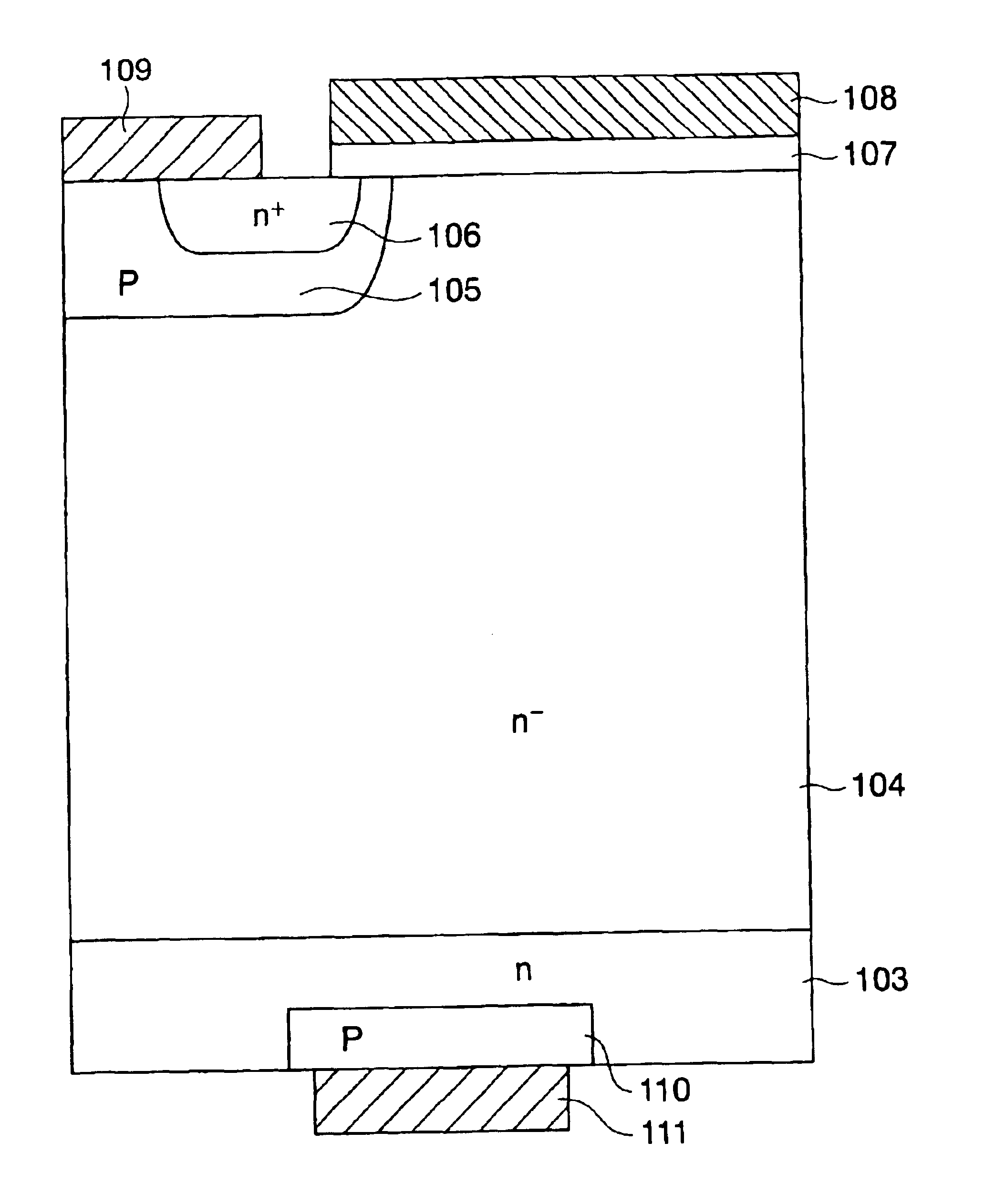
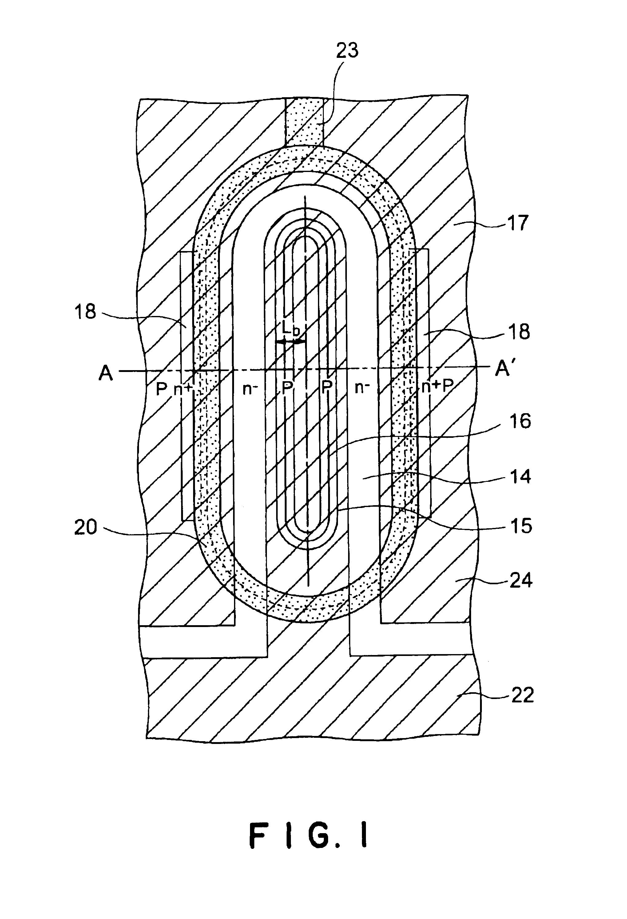
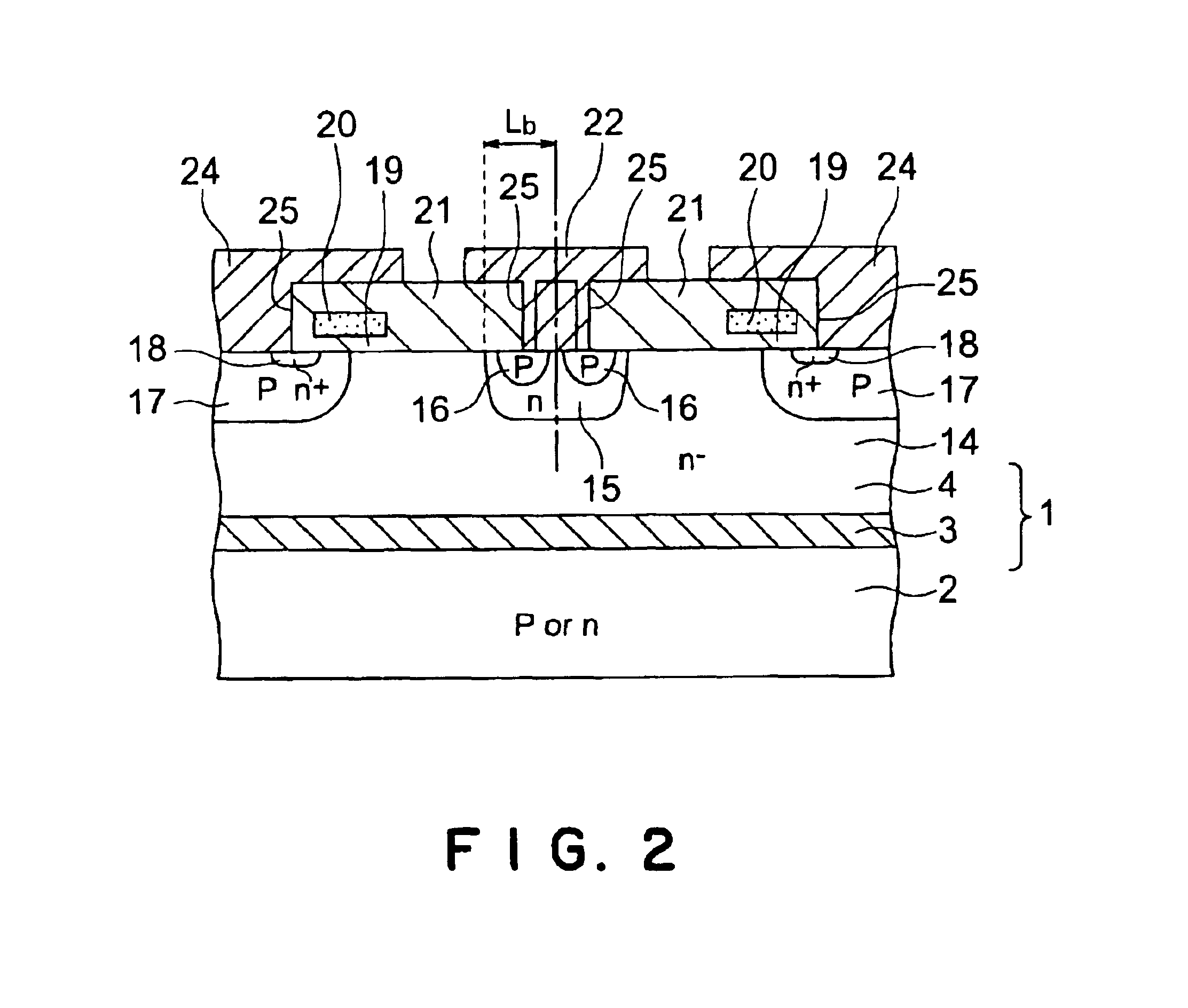
[0060]FIG. 1 is a plan view schematically showing a lateral IGBT according to the first embodiment of the present invention. FIG. 2 is a sectional view taken along a line A-A′ in FIG. 1.

[0061]An SOI substrate 1 has a silicon support substrate 2, a buried oxide film 3, and a high-resistance, n−-type silicon active layer 4. In the IGBT of this embodiment, the n−-type silicon active layer 4 is used as an n−-type base layer 14. An n-type buffer layer 15 is formed in the surface of the n−-type base layer 14 by selective diffusion. This n-type buffer layer 15 has a stripe shape whose two, upper and lower end portions protrude outward into the shape of an arc having a curvature R. A p-type drain layer 16 is formed in the surface of the n-type buffer layer 15 by selective diffusion.

[0062]In this embodiment, the p-type drain layer 16 has the same shape as the n-type buffer layer 15 and has an annular structure.

[0063]In the surface of the n−-type base layer 14, a p-type base laye

Example

Second Embodiment

[0070]FIG. 3 is a plan view of a lateral IGBT according to the second embodiment of the present invention. A sectional view taken along a line A-A′ in FIG. 3 is the same as FIG. 2, so this sectional view will be omitted.

[0071]A difference of this embodiment from the above first embodiment is that in the first embodiment the p-type drain layer 16 has an annular structure, but in this embodiment a p-type drain layer 36 has a horseshoe-shaped or inverse U-shaped structure formed by cutting away in the horizontal direction (a lateral direction on the paper surface) one of the upper and lower end portions, e.g., the lower end portion of the p-type drain layer 16 having the annular structure in the first embodiment. The rest of the arrangement is the same as the first embodiment.

[0072]In the lateral IGBT of this embodiment, the area of the p-type drain layer 36 is smaller than the aforementioned IGBT related to the present invention. As in the first embodiment described abov

Example

Third Embodiment

[0076]FIG. 6 is a plan view of a lateral IGBT according to the third embodiment of the present invention. A sectional view taken along a line A-A′ in FIG. 6 is the same as FIG. 2, so this sectional view will be omitted.

[0077]A difference of this embodiment from the above first embodiment is that in the first embodiment the p-type drain layer 16 has an annular structure, but in this embodiment p-type drain layers 46 are two striped structures formed by cutting away in the horizontal direction the upper and lower end portions of the p-type drain layer 16 having the annular structure in the first embodiment. The rest of the arrangement is the same as the first embodiment.

[0078]In the lateral IGBT of this embodiment, the area of the p-type drain layers 46 is smaller than that in the aforementioned IGBT related to the present invention. As in the first embodiment described above, therefore, the breakdown voltage can be raised without raising the ON voltage.

[0079]Also, the p-


PUM


Abstract

A vertical semiconductor device including a first conductivity type base layer having resistance higher then of a first conductivity type buffer layer, the first conductivity type buffer layer formed in one surface portion of the first conductivity type base layer, a second conductivity type drain layer selectively formed in a surface portion of the first conductivity type buffer layer, a second conductivity type base layer selectively formed in the other surface portion of the first conductivity type base layer, a first conductivity type source layer selectively formed in a surface portion of the second conductivity type base layer, a gate insulating film formed on the second conductivity type base layer between the first conductivity type source layer and the first conductivity type base layer, a gate electrode formed on the second conductivity type base layer via the gate insulating film, a drain electrode electrically connected to the second conductivity type drain layer, and a source electrode electrically connected to the first conductivity type source layer and the second conductivity type base layer, wherein the drain electrode is not electrically connected to the first conductivity buffer layer.

Description


Claims


Application Information

Patent Timeline
Owner KK TOSHIBA
Why Eureka
Try Eureka