Ultrathin shadow mask type plasma display screen
A plasma and display technology, applied in the direction of solid cathode components, cold cathode tubes, etc., can solve the problems of low production efficiency, high production cost, heavy weight, etc., achieve light overall weight, reduce overall weight, and simplify the manufacturing process Effect
- Summary
- Abstract
- Description
- Claims
- Application Information
AI Technical Summary
Benefits of technology
Problems solved by technology
Method used
Image

Examples
Embodiment 1
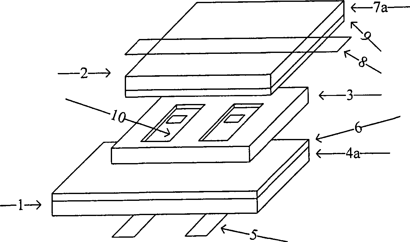
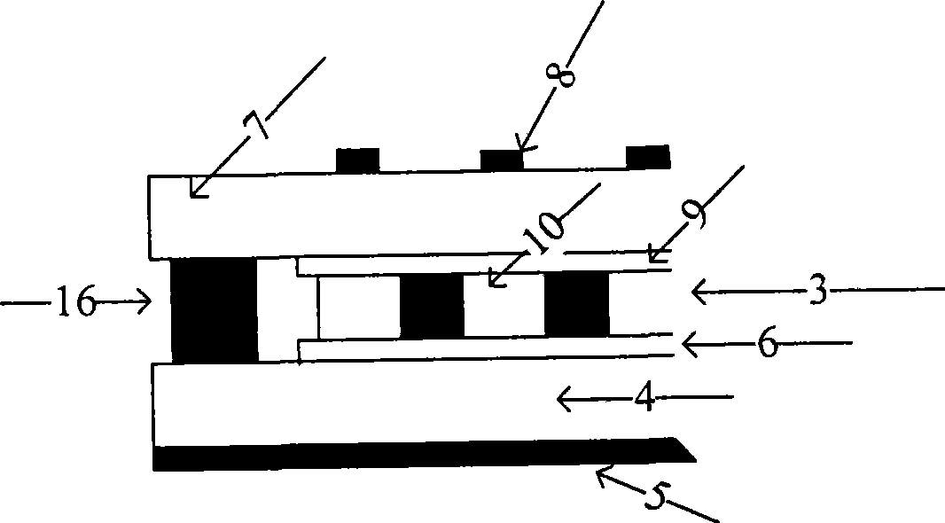
[0025]The ultra-thin shadow mask type plasma display screen of the present invention, as shown in FIG. 1 , consists of a rear substrate 1 , a front substrate 2 and a shadow mask 3 . The rear substrate 1 is composed of a rear substrate glass substrate 4a, a protective film 6 and a first electrode 5, that is, an address electrode or a column electrode. The thickness of the rear substrate glass substrate 4a is 10 μm-100 μm. Form the first electrode 5, commonly referred to as column electrode or address electrode, and form protective film 6 on the inner surface of back substrate glass substrate 4a; Front substrate 2 comprises front substrate glass substrate 7a, protective film 9 and second electrode 8 namely For scanning electrodes or row electrodes, the thickness of the front substrate glass substrate 7a is 10 μm-100 μm, and the second electrode 8 is formed on the outer surface of the front substrate glass substrate 7a in a space perpendicular to the first electrode 5, which is usual
Embodiment 2
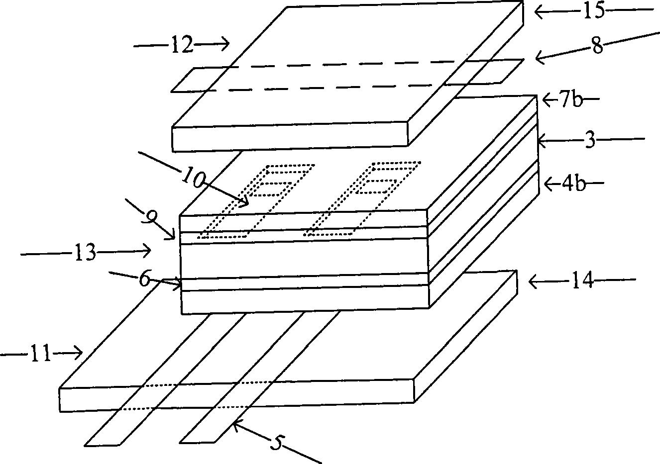
[0027] Ultra-thin shadow mask type plasma display screen of the present invention, as figure 2 As shown, it is composed of a rear substrate 11, a front substrate 12 and a gas box 13. It is characterized in that the rear substrate substrate 14 and the front substrate substrate 15 are glass or soft base material films with a thickness of 0.01-1 mm, and the rear substrate 11 is made of a rear substrate. The base substrate 14 and the first electrode 5 are address electrodes or column electrodes. The inner surface of the back substrate substrate 14 is provided with the first electrode 5; the front substrate 2 is composed of the front substrate substrate 15 and the second electrode 8, which is the scanning electrode. or row electrodes, the inner surface of the front substrate substrate 15 is provided with a second electrode 8, the second electrode 8 and the first electrode 5 are vertically orthogonal in space; the gas box 13 is sandwiched between the front substrate 2 and the rear subs
Embodiment 3
[0029] In the first embodiment above, instead of coating the walls of the grid holes 10 of the shadow mask 3 with ultraviolet-excited phosphors, the grid holes 10 arrays of the shadow mask 3 are coated with red, green, and blue primary-color ultraviolet-excited phosphors sequentially. , so that the ultraviolet light of the corresponding wavelength excites the ultraviolet phosphor to emit red, green and blue primary color visible light, and then the color image can be displayed, which constitutes a colorful ultra-thin shadow mask plasma display.
PUM
| Property | Measurement | Unit |
|---|---|---|
| Thickness | aaaaa | aaaaa |
| Thickness | aaaaa | aaaaa |
| Thickness | aaaaa | aaaaa |
Abstract
Description
Claims
Application Information
 - R&D Engineer
- R&D Manager
- IP Professional
- Industry Leading Data Capabilities
- Powerful AI technology
- Patent DNA Extraction
Browse by: Latest US Patents, China's latest patents, Technical Efficacy Thesaurus, Application Domain, Technology Topic.
© 2024 PatSnap. All rights reserved.Legal|Privacy policy|Modern Slavery Act Transparency Statement|Sitemap