PWM/PDM double-mode modulation selective circuit and double-mode modulation method
A technology for selecting circuits and modulation modes, applied in the field of microelectronics, can solve the problems of difficult implementation, complex circuits, high cost, etc., achieve high average conversion efficiency, simple circuit structure, and reduce application costs
- Summary
- Abstract
- Description
- Claims
- Application Information
AI Technical Summary
Benefits of technology
Problems solved by technology
Method used
Image

Examples
Embodiment Construction
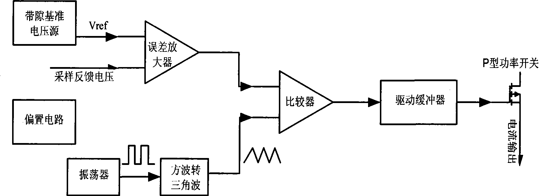
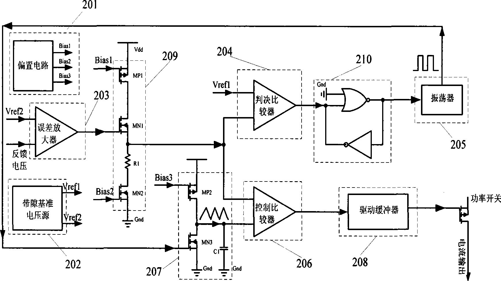
[0027] refer to figure 2 , a PWM / PDM dual-mode modulation selection circuit of the present invention includes: bias circuit 201, bandgap reference voltage source 202, error amplifier 203, mode decision comparator 204, oscillator 205, control comparator 206, integrator 207 , drive buffer 208 , latch 210 and isolated source follower 209 . in:
[0028] The isolated source follower 209 is composed of PMOS transistor MP1, NMOS transistor MN1, resistor R1 and NMOS transistor MN2 connected in series. The gate of MN1 is the input and the drain is the output. Integrator 207 is composed of MN3 connected in parallel with capacitor C1 and then connected in series with MP2, the signal is input from the gate of MN3 and output from the drain. The latch 210 is composed of a NOR gate coupled with an inverter. The bias circuit 201 provides three bias voltages Bias1, Bias2 and Bias3 for the entire loop, and the bandgap reference voltage source 202 generates two reference voltages Vref1 and Vr
PUM
 Abstract
Description
Claims
Application Information
 - R&D Engineer
- R&D Manager
- IP Professional
- Industry Leading Data Capabilities
- Powerful AI technology
- Patent DNA Extraction
Browse by: Latest US Patents, China's latest patents, Technical Efficacy Thesaurus, Application Domain, Technology Topic.
© 2024 PatSnap. All rights reserved.Legal|Privacy policy|Modern Slavery Act Transparency Statement|Sitemap