DC offset correction circuit and method

A DC offset and correction circuit technology, applied in the direction of DC coupled DC amplifiers, differential amplifiers, etc., can solve the problem of slow signal response rate, etc., and achieve the effect of reducing circuit area and complexity

Inactive Publication Date: 2009-07-29
IND TECH RES INST
View PDF1 Cites 12 Cited by
  • Summary
  • Abstract
  • Description
  • Claims
  • Application Information

AI Technical Summary

Benefits of technology

This patented technology allows for accurate detection of voltage differences between two circuits without any issues with their consistency or dispersion problem. It also includes techniques like binary searching and approximate approximations to determine how much correction needs to be done based on certain factors such as temperature and power supply levels. By reducing this process, it makes the overall design more efficient while still maintaining accuracy over different conditions.

Problems solved by technology

Technological Problem: Direct Conversion Systems have been developed due to their small size and multiple modes capabilities compared to other types such as Super Heteroardnership Modulation System (SHM). However, there may still exist some challenges related to reducing the number of required parts while maintaining desired performance levels. These issues include improving linearity without increasing power consumption, minimizing interference from external sources like electromagnetic waves, eliminating distortion effects during transmission over long distances, achieving higher efficiency at lower frequencies, etc., which requires more complex hardware solutions.

Method used


Image

  • DC offset correction circuit and method
  • DC offset correction circuit and method
  • DC offset correction circuit and method

Examples


Embodiment Construction

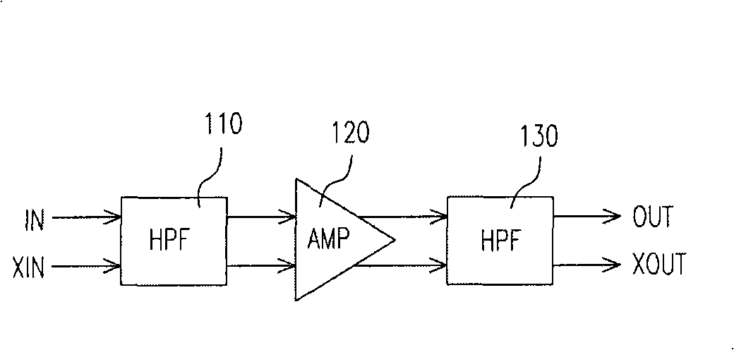
[0048] The traditional DC offset correction circuit uses a multi-bit analog-to-digital converter to detect the DC offset part of the output signal to update the compensation value of the DC offset. The DC offset correction circuit and method of the present invention adopt a step-by-step approach to obtain only one bit of the compensation value at a time, and when all bits of the compensation value (for example, 8 bits) are set and updated, it is calculated Obtain the correct value of DC offset compensation. In order to make the content of the present invention more clear, the following embodiments are specifically cited as examples on which the present invention can be implemented.

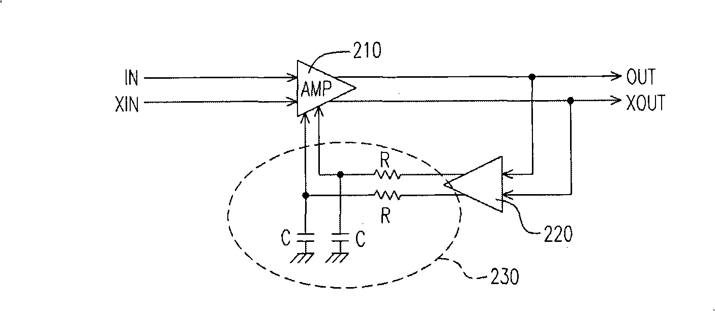
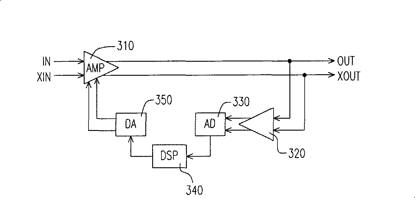
[0049] Figure 4 It is a circuit diagram of DC offset correction according to an embodiment of the present invention. Please refer to Figure 4 The DC offset correction circuit 400 of this embodiment is used to correct the DC offset in the output signal output by the signal processing unit 410. The sign


PUM


Abstract

The invention discloses a circuit and a method for correcting the direct current (DC) offset part in output signals of a signal processing unit. The DC offset correcting circuit comprises a 1 bit quantizer, a control logic unit and a digital-to-analog converter, wherein, the 1 bit quantizer is coupled to the output terminal of the signal processing unit and used for receiving and detecting the DC offset part in the output signals so as to obtain quantitative information. The control logic unit is coupled to the 1 bit quantizer and used for sequentially setting one of a plurality of bits of a compensation value and updating the set bit according to the quantitative information. The digital-to-analog converter is coupled to the control logic unit and used for compensating the DC offset part in the output signals of the signal processing unit according to the compensation value.

Description


Claims


Application Information

Patent Timeline
Owner IND TECH RES INST
Why Eureka
Try Eureka