Liquid crystal display panel and method for making substrate thereof
A technology for a liquid crystal display panel and a manufacturing method, which is applied to semiconductor/solid-state device manufacturing, static indicators, optics, etc., can solve problems such as alignment errors, process errors, and alignment errors that are prone to occur, and ensure alignment accuracy. Effect
- Summary
- Abstract
- Description
- Claims
- Application Information
AI Technical Summary
Benefits of technology
Problems solved by technology
Method used
Image

Examples
Embodiment Construction
[0026] The following descriptions of the various embodiments refer to the accompanying drawings to illustrate specific embodiments in which the present invention can be practiced. The directional terms mentioned in the present invention, such as "up", "down", "front", "back", "left", "right", "inside", "outside", "side", etc., are for reference only The orientation of the attached schema. Therefore, the directional terms used are used to illustrate and understand the present invention, but not to limit the present invention.
[0027] In the following embodiments, the same parts are denoted by the same symbols in different drawings.
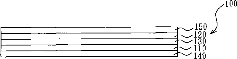
[0028] Please refer to figure 1 , which shows a schematic cross-sectional view of a liquid crystal display panel according to an embodiment of the present invention. The liquid crystal display panel 100 of this embodiment can be combined with a backlight module (not shown), and thus can be assembled into a liquid crystal display device (LCD). Suc
PUM
 Abstract
Description
Claims
Application Information
 - R&D Engineer
- R&D Manager
- IP Professional
- Industry Leading Data Capabilities
- Powerful AI technology
- Patent DNA Extraction
Browse by: Latest US Patents, China's latest patents, Technical Efficacy Thesaurus, Application Domain, Technology Topic.
© 2024 PatSnap. All rights reserved.Legal|Privacy policy|Modern Slavery Act Transparency Statement|Sitemap