Method and machine for scanning wafer defects, wafer defect scanning machine

A defect scanning and wafer technology, applied in the direction of optical testing flaws/defects, etc., can solve the problems of abnormal line width of fixed points, difficult to capture, etc., to achieve the effect of strengthening the ability to capture defects and improving the ability to capture

Active Publication Date: 2013-01-23
SHANGHAI HUALI MICROELECTRONICS CORP
View PDF5 Cites 11 Cited by
  • Summary
  • Abstract
  • Description
  • Claims
  • Application Information

AI Technical Summary

Problems solved by technology

However, when this scanning method is abnormal for the entire wafer, that is, the fifth pixel 105 is compared with the fourth pixel 104 and the sixth pixel 106. At this time, since the unit pixels adjacent to the fifth pixel 105 all Abnorm

Method used


Image

  • Method and machine for scanning wafer defects, wafer defect scanning machine
  • Method and machine for scanning wafer defects, wafer defect scanning machine
  • Method and machine for scanning wafer defects, wafer defect scanning machine

Examples


Embodiment Construction

[0020] The present invention is described below in conjunction with embodiment.

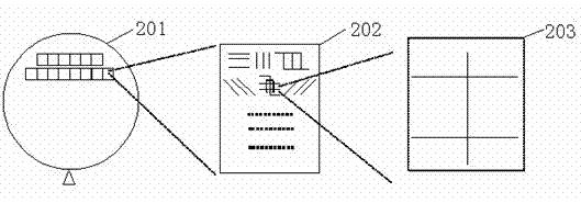
[0021] figure 2 The relationship between the unit pixel 203 , the wafer 201 and the unit chip 202 mentioned in the embodiment of the present invention is shown.

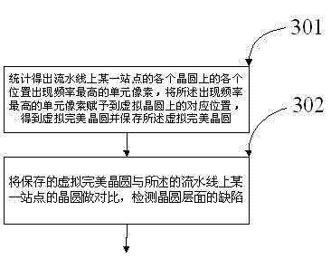
[0022] Such as image 3 As shown in the flow chart of the present invention, the steps of the wafer defect scanning method in the embodiment of the present invention include:

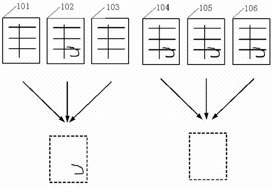
[0023] In step 301, the unit pixel with the highest frequency of occurrence at each position on each wafer of a certain station on the assembly line is counted, and the unit pixel with the highest frequency of occurrence is assigned to the corresponding position on the virtual wafer to obtain a virtual perfect wafer And save the virtual perfect wafer; the wafers passing through a certain station on the wafer processing line should have consistent morphological characteristics, so it is meaningful to carry out statistics at the same station, and the morphologies a


PUM


Abstract

The invention discloses a method for scanning wafer defects, which comprises the steps of: calculating to obtain the most frequent unit pixels of various positions on various wafers of some station on a production line and applying to corresponding positions on a virtual wafer to obtain a virtual perfect wafer, and storing the virtual perfect wafer; comparing the stored virtual perfect wafer with the wafer of some station on the production line; and detecting defects of the wafer layer. Furthermore, the invention discloses a machine for scanning wafer defects, including the method for scanning wafer defects. According to the scanning method, a defect scanning way of comparing the virtual perfect wafer and the wafer is added, thereby enhancing the ability of the scanning machine to catch the defects.

Description


Claims


Application Information

Patent Timeline
Owner SHANGHAI HUALI MICROELECTRONICS CORP
Why Eureka
Try Eureka