Forming method of semiconductor structure, and semiconductor structure

A technology of semiconductor and isolation structure, applied in the field of semiconductor structure formation method and semiconductor structure, can solve the problems of occupying a large chip area and the shallow trench isolation structure cannot continue to shrink, and achieves the reduction of occupied area, size, and size. Effect of Trigger Voltage

Inactive Publication Date: 2014-07-16
SEMICON MFG INT (SHANGHAI) CORP
View PDF6 Cites 0 Cited by
  • Summary
  • Abstract
  • Description
  • Claims
  • Application Information

AI Technical Summary

Problems solved by technology

[0008] The problem solved by the present invention is that the shallow trench isolation st

Method used


Image

  • Forming method of semiconductor structure, and semiconductor structure
  • Forming method of semiconductor structure, and semiconductor structure
  • Forming method of semiconductor structure, and semiconductor structure

Examples


Embodiment Construction

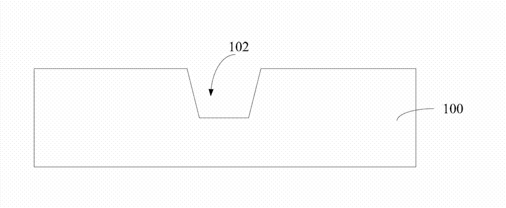
[0046] The inventors have found and analyzed that the reason why the shallow trench isolation structure in the prior art cannot continue to shrink and occupy a large area of ​​the chip is as follows:

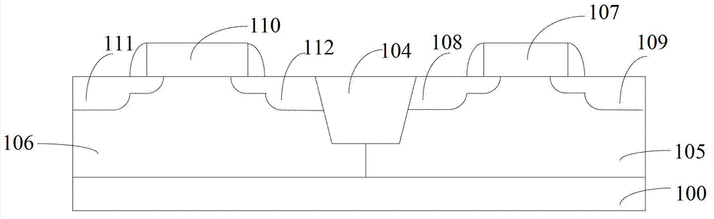
[0047] refer to image 3 , in the prior art, the holes in the P well region 106 will diffuse to the N well region 105, and the electrons in the N well region 105 will diffuse to the P well region 106. Therefore, the holes diffused to the N well region 105 and diffused to the P The electrons in the well region 106 will recombine at the bottom of the shallow trench isolation structure 104 to form a depletion region. When the device works, it is necessary to apply a voltage to the source and drain of the PMOS transistor and the NMOS transistor, and the width of the depletion region will increase under the effect of the applied voltage. If the size of the shallow trench isolation structure 104 is reduced at this time, it is equivalent to Narrowing the distance between the drain 112 of


PUM


Abstract

The invention provides a forming method of a semiconductor structure, and a semiconductor structure. The forming method of the semiconductor structure comprises: forming a groove in a substrate, the groove dividing the substrate into a first active area and a second active area; forming a first well region in the first active area, forming a second well region in the second active area, and forming a depletion region at the connection position of the first well region and the second well region; performing first ion implantation in the first well region at the bottom of the groove, and performing second ion implantation in the second well region at the bottom of the groove, the type of the first ion implantation being the same as the type of the first well region, the type of the second ion implantation being the same as the type of the second well region; and after the ion implantation, filling a dielectric layer in the groove to form an isolation structure. According to the invention, the method reduces the dimension of the isolation structure and accordingly reduces the occupation area of the isolation structure on a chip; a electrostatic protection circuit can also be quite easily triggered so as to protect a semiconductor device from being damaged; and the latch effect generation probability can also be reduced.

Description


Claims


Application Information

Patent Timeline
Owner SEMICON MFG INT (SHANGHAI) CORP
Why Eureka
Try Eureka