Spot measurement equipment of light emitting diode chip
A light-emitting diode and chip technology, applied in the semiconductor field, can solve the problem of high implementation cost and achieve the effect of improving accuracy
- Summary
- Abstract
- Description
- Claims
- Application Information
AI Technical Summary
Problems solved by technology
Method used
Image

Examples
Embodiment Construction
[0036] In order to make the object, technical solution and advantages of the present invention clearer, the implementation manner of the present invention will be further described in detail below in conjunction with the accompanying drawings.
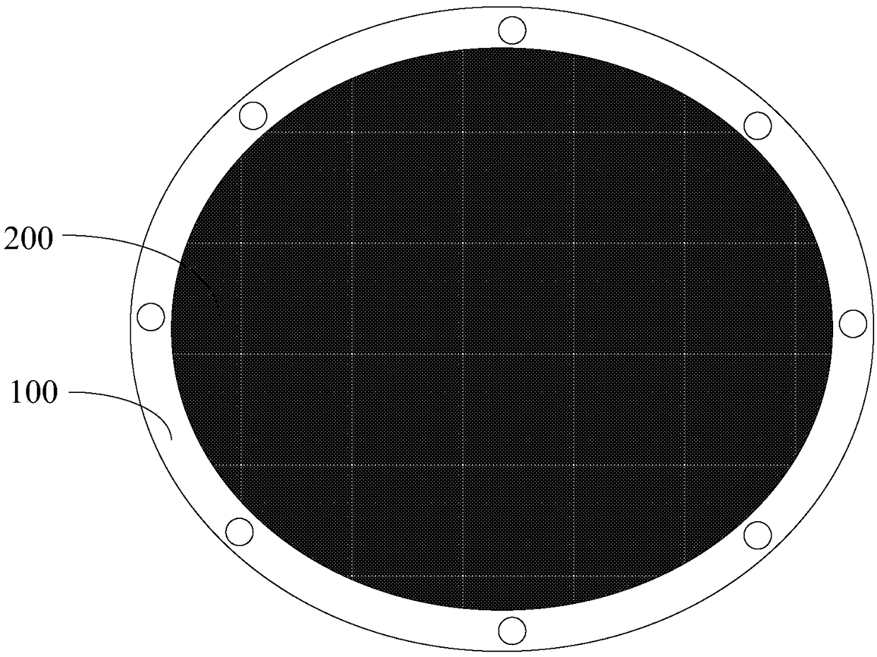
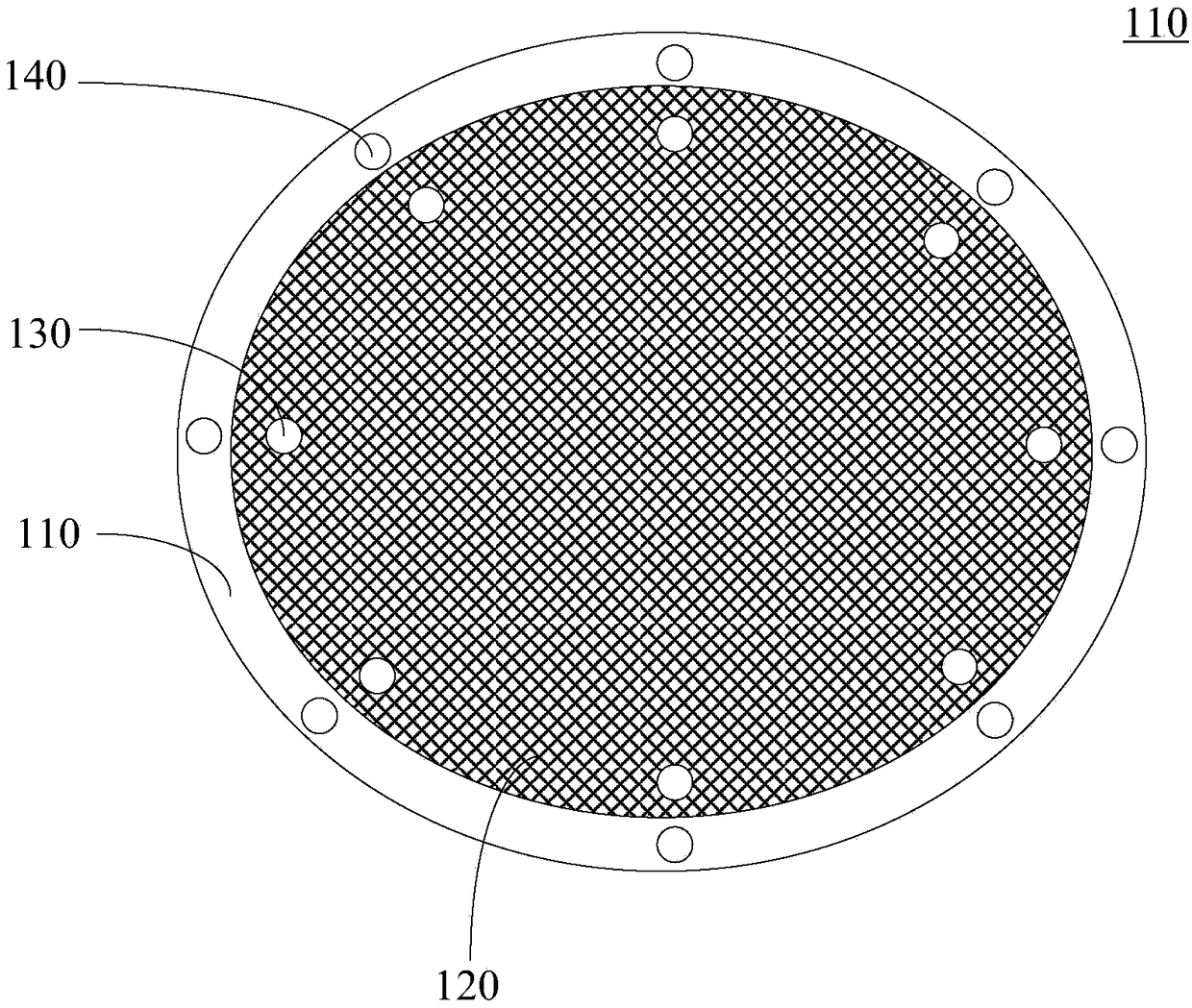
[0037] An embodiment of the present invention provides a light-emitting diode chip point measurement device, figure 1 It is a partial structural schematic diagram of a point-testing device for a light-emitting diode chip provided by an embodiment of the present invention, as shown in figure 1 As shown, the wafer stage device includes a wafer receiver device 100, an optical path conversion device 200 and a light receiving device (not shown in the figure).
[0038] The chip carrier device 100 is used for carrying LED chips (not shown in the figure).
[0039] The optical path conversion device 200 is arranged between the substrate device 100 and the LED chip, and is used to reflect the light emitted from the LED chip to the substrate dev...
PUM
 Abstract
Description
Claims
Application Information
 - R&D Engineer
- R&D Manager
- IP Professional
- Industry Leading Data Capabilities
- Powerful AI technology
- Patent DNA Extraction
Browse by: Latest US Patents, China's latest patents, Technical Efficacy Thesaurus, Application Domain, Technology Topic.
© 2024 PatSnap. All rights reserved.Legal|Privacy policy|Modern Slavery Act Transparency Statement|Sitemap