Display panel and display device
A display panel and display device technology, applied in nonlinear optics, instruments, optics, etc., can solve problems such as destroying QD material particles and affecting material properties
- Summary
- Abstract
- Description
- Claims
- Application Information
AI Technical Summary
Benefits of technology
Problems solved by technology
Method used
Image

Examples
Embodiment Construction
[0030] Please refer to the drawings in the accompanying drawings, wherein like reference numerals refer to like components. The following description is based on illustrated specific embodiments of the present application, which should not be construed as limiting other specific embodiments of the present application that are not described in detail here.
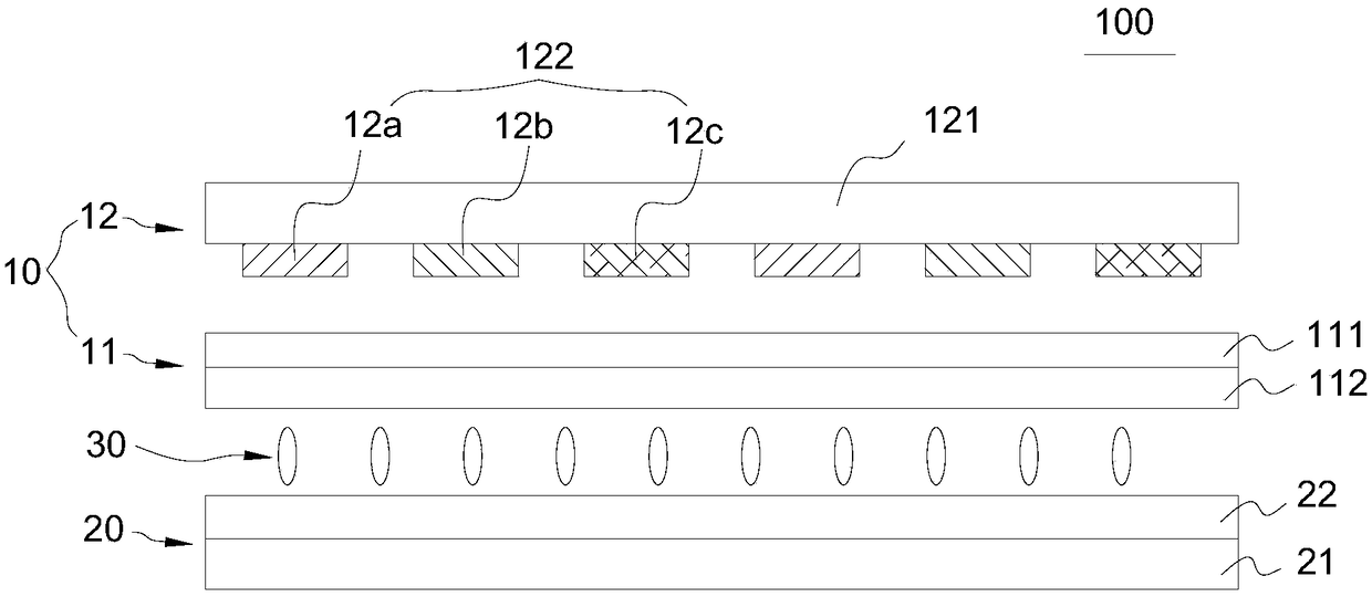
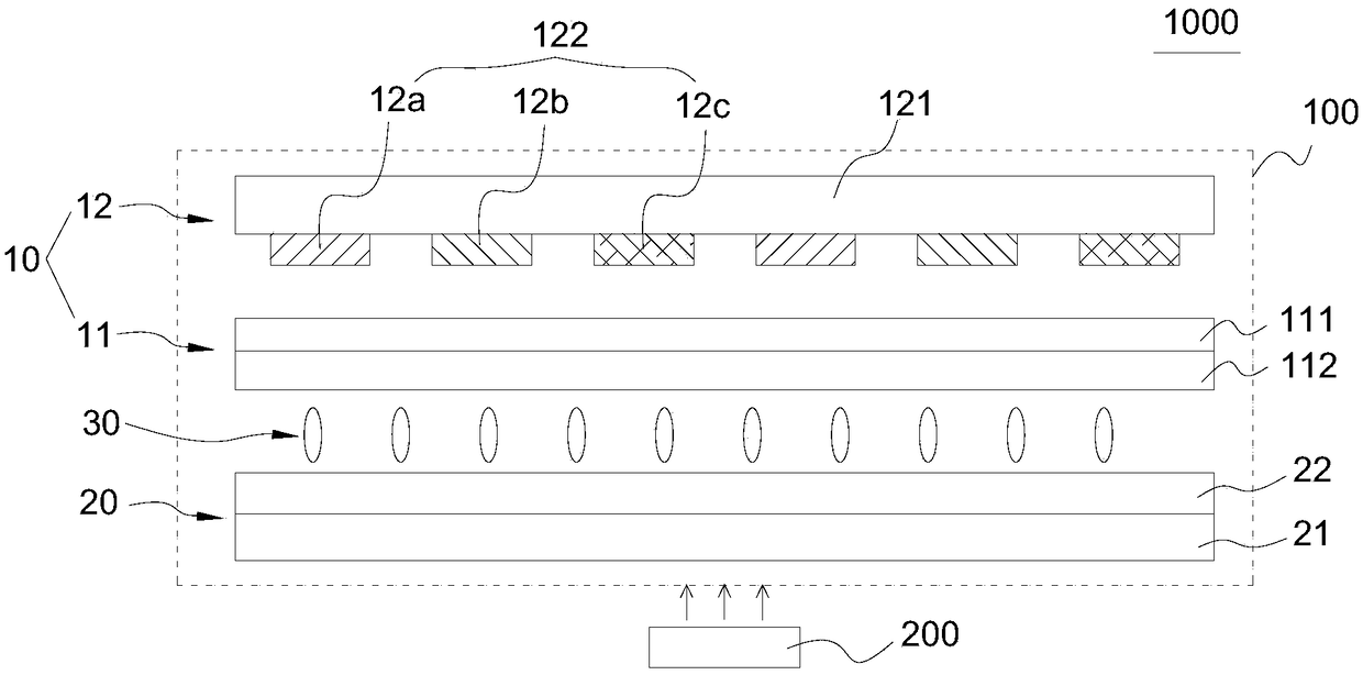
[0031] Please refer to figure 2 , figure 2 It is a structural schematic diagram of an embodiment of the display panel of the present application. The display panel 100 of the embodiment of the present application includes a color filter structure 10 , an array substrate 20 and a liquid crystal layer 30 disposed between the color filter structure 10 and the array substrate 20 .
[0032] The color filter structure 10 includes a first substrate 11 and a second substrate 12 . The first substrate 11 is disposed on the liquid crystal layer 30 and is used to provide voltage to the liquid crystal layer 30 and cooperate with the e
PUM
 Abstract
Description
Claims
Application Information
 - R&D Engineer
- R&D Manager
- IP Professional
- Industry Leading Data Capabilities
- Powerful AI technology
- Patent DNA Extraction
Browse by: Latest US Patents, China's latest patents, Technical Efficacy Thesaurus, Application Domain, Technology Topic.
© 2024 PatSnap. All rights reserved.Legal|Privacy policy|Modern Slavery Act Transparency Statement|Sitemap