Optical touch device
An optical touch and light sensing technology
- Summary
- Abstract
- Description
- Claims
- Application Information
AI Technical Summary
Benefits of technology
Problems solved by technology
Method used
Image

Examples
Embodiment Construction
[0031] Below in conjunction with accompanying drawing, structural principle and working principle of the present invention are specifically described:
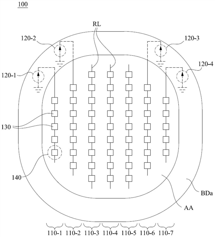
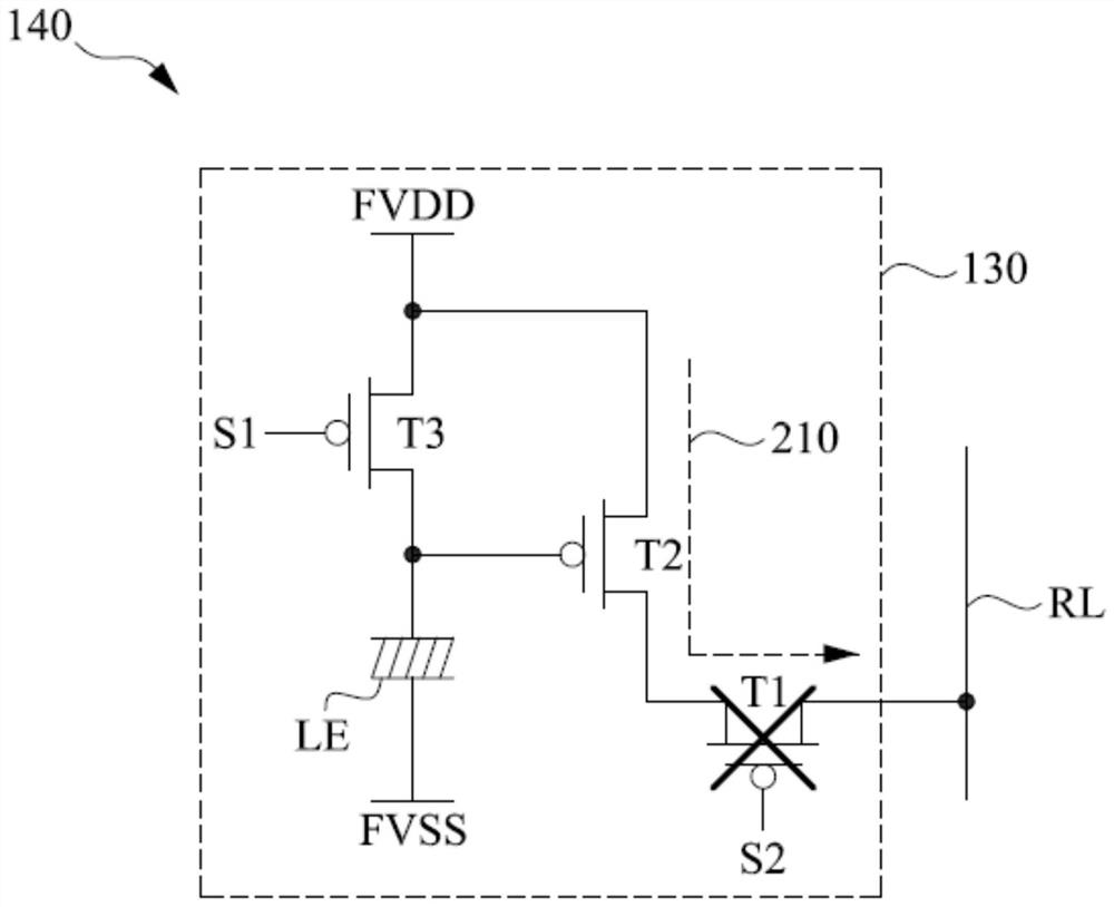
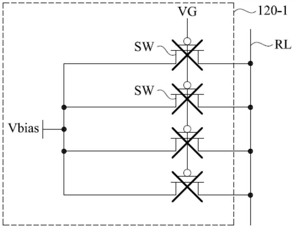
[0032] figure 1 It is a simplified functional block diagram of the optical touch device 100 according to an embodiment of the present invention. The optical touch device 100 includes a plurality of light-sensing pixel columns 110-1-110-7, a plurality of compensation current sources 120-1-120-4, and a plurality of readout lines RL. Each of the light-sensing pixel columns 110-1˜110-7 includes a plurality of light-sensing pixels 130 commonly coupled to a corresponding readout line RL. In some embodiments, the optical touch device 100 may include a plurality of scanning lines and a scanning driving circuit for enabling the photo-sensing pixels 130 column by column, and may also include a scanning result for reading the photo-sensing pixels 130 Multiple readout circuits (such as integrators), may also include display modules, for th
PUM
 Abstract
Description
Claims
Application Information
 - R&D Engineer
- R&D Manager
- IP Professional
- Industry Leading Data Capabilities
- Powerful AI technology
- Patent DNA Extraction
Browse by: Latest US Patents, China's latest patents, Technical Efficacy Thesaurus, Application Domain, Technology Topic.
© 2024 PatSnap. All rights reserved.Legal|Privacy policy|Modern Slavery Act Transparency Statement|Sitemap