Vertical field effect transistor formation with critical dimension control

a technology of vertical field effect transistor and critical dimension control, which is applied in the direction of basic electric elements, electrical apparatus, and semiconductor devices. it can solve the problems of corresponding increase in short channel effects and vfet performance variations

Active Publication Date: 2019-02-26
GLOBALFOUNDRIES US INC
View PDF15 Cites 12 Cited by
  • Summary
  • Abstract
  • Description
  • Claims
  • Application Information

AI Technical Summary

Benefits of technology

This patented describes methods that allow for controllable formation of small devices called Vertically Field Effect Transistor (VFT' s) by depositing specific materials onto certain areas within an insulating film made from silica glass. These techniques help create smaller electronic components such as switch elements and sensory chips.

Problems solved by technology

This patented technical problem addressed in this patents relates to improving the process used during integrated circuit fabrication due to factors like shrinking dimensions caused by miniaturization or high integration densities. These issues lead to increased variabilities in device characteristics and reduced overall productivity rates while also increasing complexity and cost associated with integrating different types of circuits into one package. There has been some progress towards achieving greater precision in controlling these parameters through various methods including lithography patterning technology, but it remains difficult to achieve consistency throughout multiple dies without compromising their quality.

Method used


Image

  • Vertical field effect transistor formation with critical dimension control
  • Vertical field effect transistor formation with critical dimension control
  • Vertical field effect transistor formation with critical dimension control

Examples


Embodiment Construction

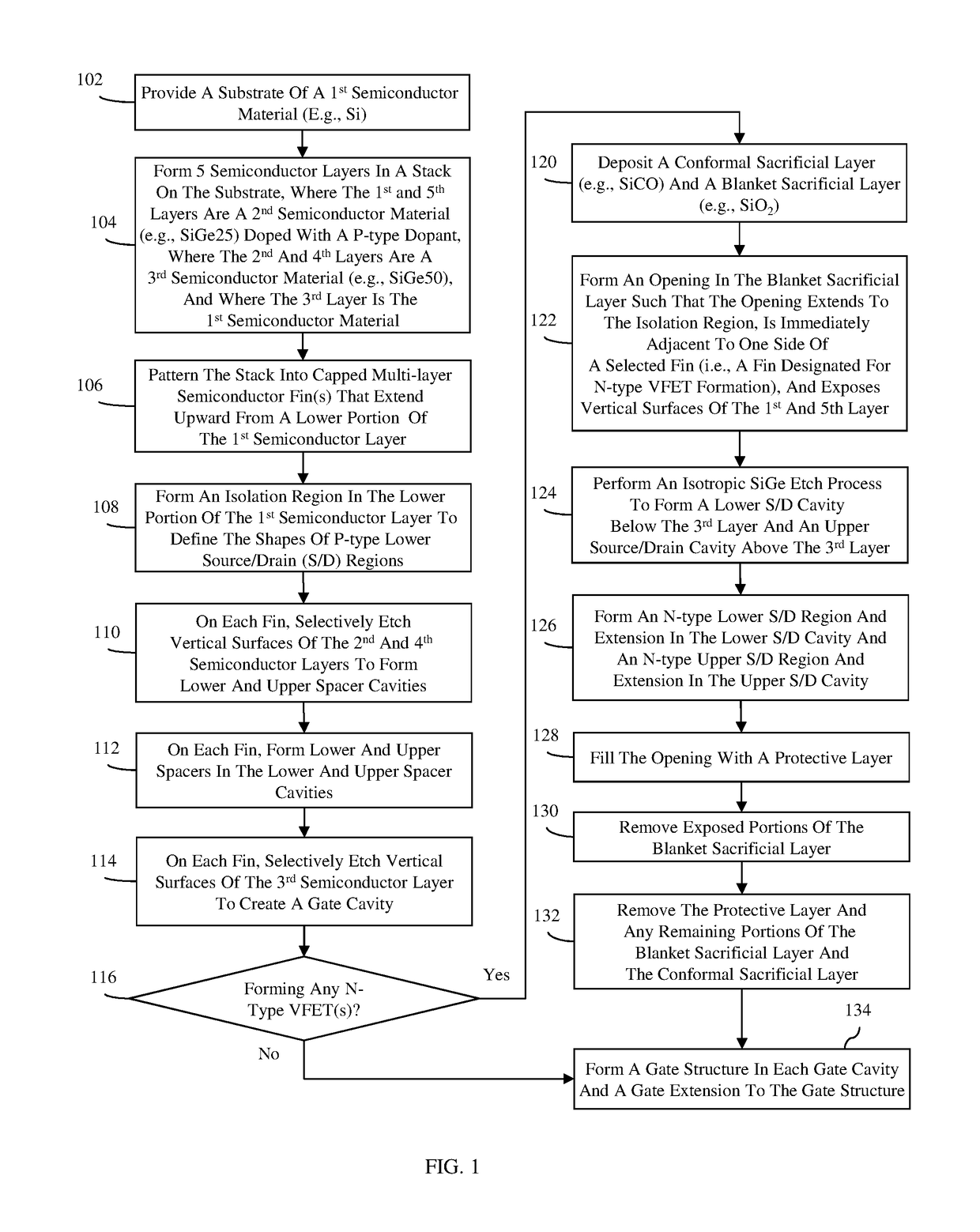
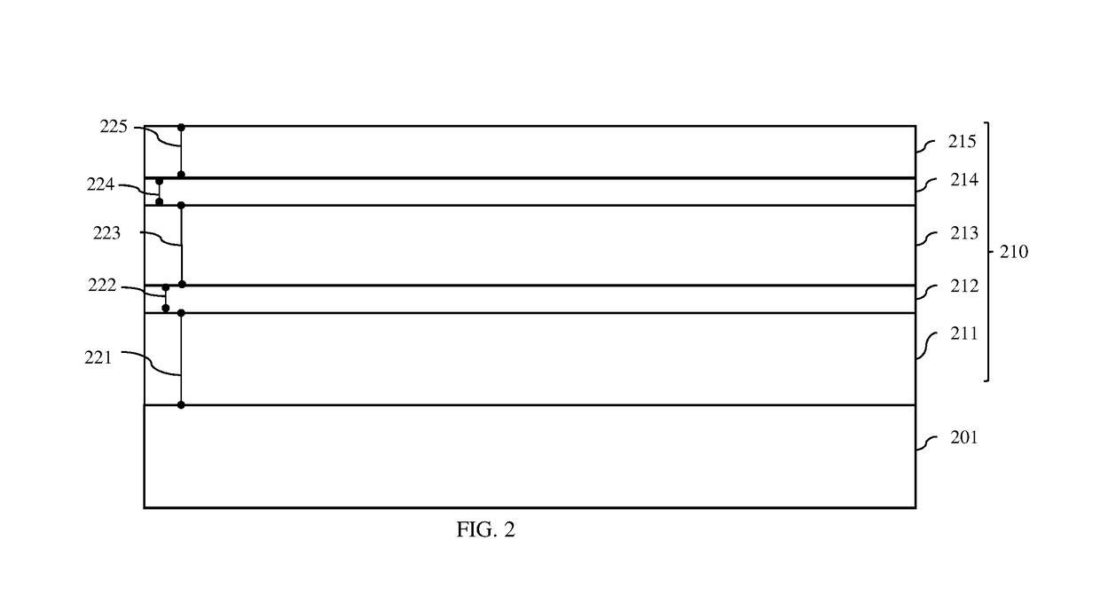
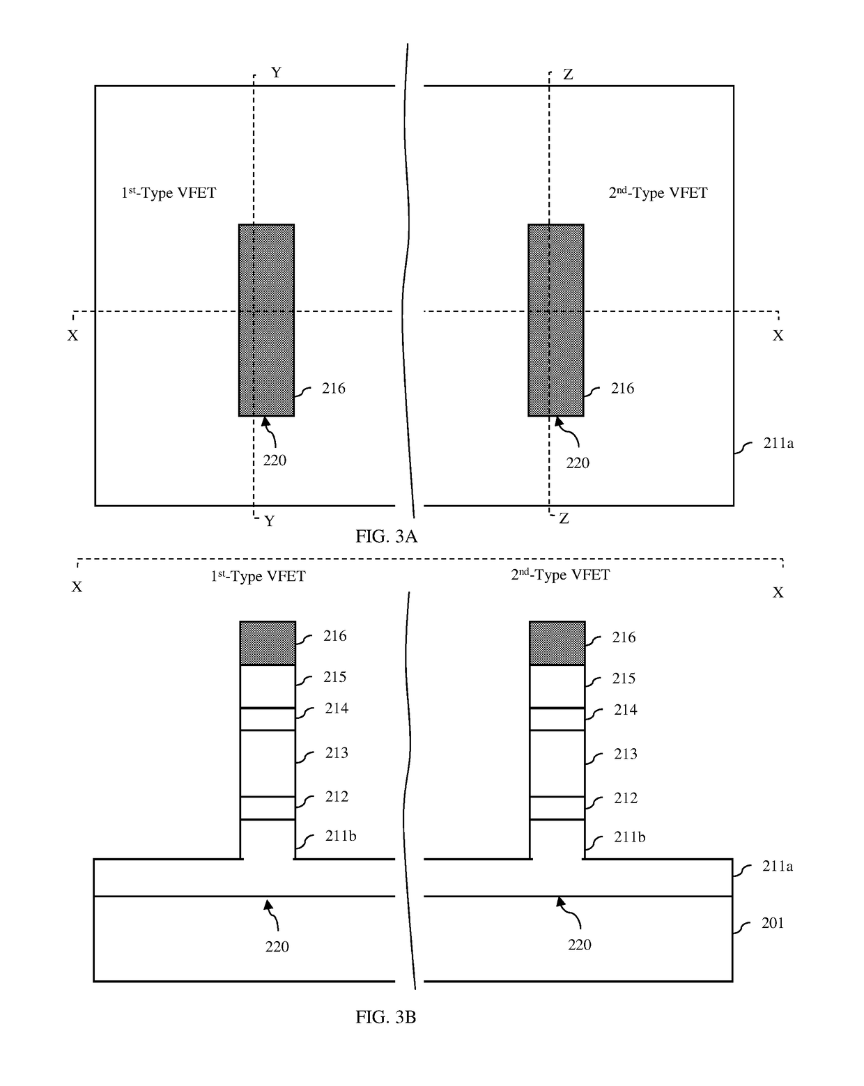
[0037]As mentioned above, as mentioned above critical dimension control (e.g., control of gate length, control of alignment of top and bottom junction doping to gate edges, etc.) can be challenging with current methods of forming vertical field effect transistors (VFETs). For example, the lengths of the lower and upper spacers, which define the spacing between the channel region and the lower and upper source / drain regions, respectively, of a VFET are achieved by depositing spacer material and then recessing the spacer material using a timed etch process. Similarly, the length of the gate of a VFET is defined by depositing sacrificial gate material and then recessing the sacrificial gate material using a timed etch process. However, those skilled in the art will recognize that there can be a lot of process variation when using timed etch processes. As a result, VFET performance variations (e.g., variations in threshold voltage) can occur.

[0038]In view of the foregoing, disclosed here


PUM


Abstract

Disclosed are a method of forming vertical field effect transistor(s) and the resulting structure. In the method, five semiconductor layers are formed in a stack by epitaxial deposition. The first and fifth layers are one semiconductor material, the second and fourth layers are another and the third layer is yet another. The stack is patterned into fin(s). Vertical surfaces of the second and fourth layers of the fin(s) are etched to form upper and lower spacer cavities and these cavities are filled with upper and lower spacers. Vertical surfaces of the third layer of the fin(s) are etched to form a gate cavity and this cavity is filled with a gate. Since epitaxial deposition is used to form the semiconductor layers, the thicknesses of these layers and thereby the heights of the spacer cavities and gate cavity and the corresponding lengths of the spacers and gate can be precisely controlled.

Description


Claims


Application Information

Patent Timeline
Owner GLOBALFOUNDRIES US INC
Why Eureka
Try Eureka