Integrated circuit with bit error test capability

a technology of integrated circuits and bit error testing, which is applied in the direction of testing circuits, instruments, process and machine control, etc., can solve problems such as adversely affecting signal performance, and achieve the effects of reducing signal influence, reducing signal influence, and increasing accuracy of bit error testing

Inactive Publication Date: 2007-07-12
KEYSIGHT TECH
View PDF5 Cites 2 Cited by
  • Summary
  • Abstract
  • Description
  • Claims
  • Application Information

AI Technical Summary

Benefits of technology

Inventors found it easier than ever before they needed to use older equipment from their own chipsets when trying to detect errors caused during manufacture. They used these new tools instead of relying solely upon specialized measurement locations at specific times throughout the chip's life. By doing things right with them, companies could save money while still being able to accurately diagnose any issues related to their products.

Problems solved by technology

This patented describes how integrating electronic devices like FPGAs can be done efficiently by combining different components together into larger systems called ASIs that work alongside each other on their own chip. These modules are designed specifically for this purpose based upon certain factors including size constraints imposed during manufacturing processes.

Method used


Image

  • Integrated circuit with bit error test capability
  • Integrated circuit with bit error test capability

Examples


Embodiment Construction

[0007] Other objects and many of the attendant advantages of the present invention will be readily appreciated and become better understood by reference to the following detailed description when considering in connection with the accompanied drawing.

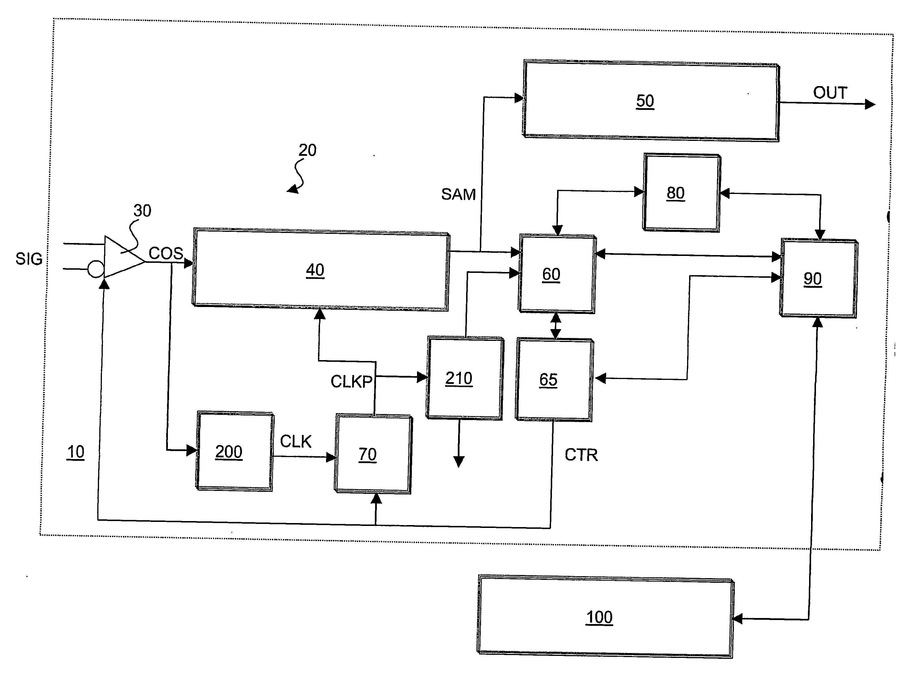
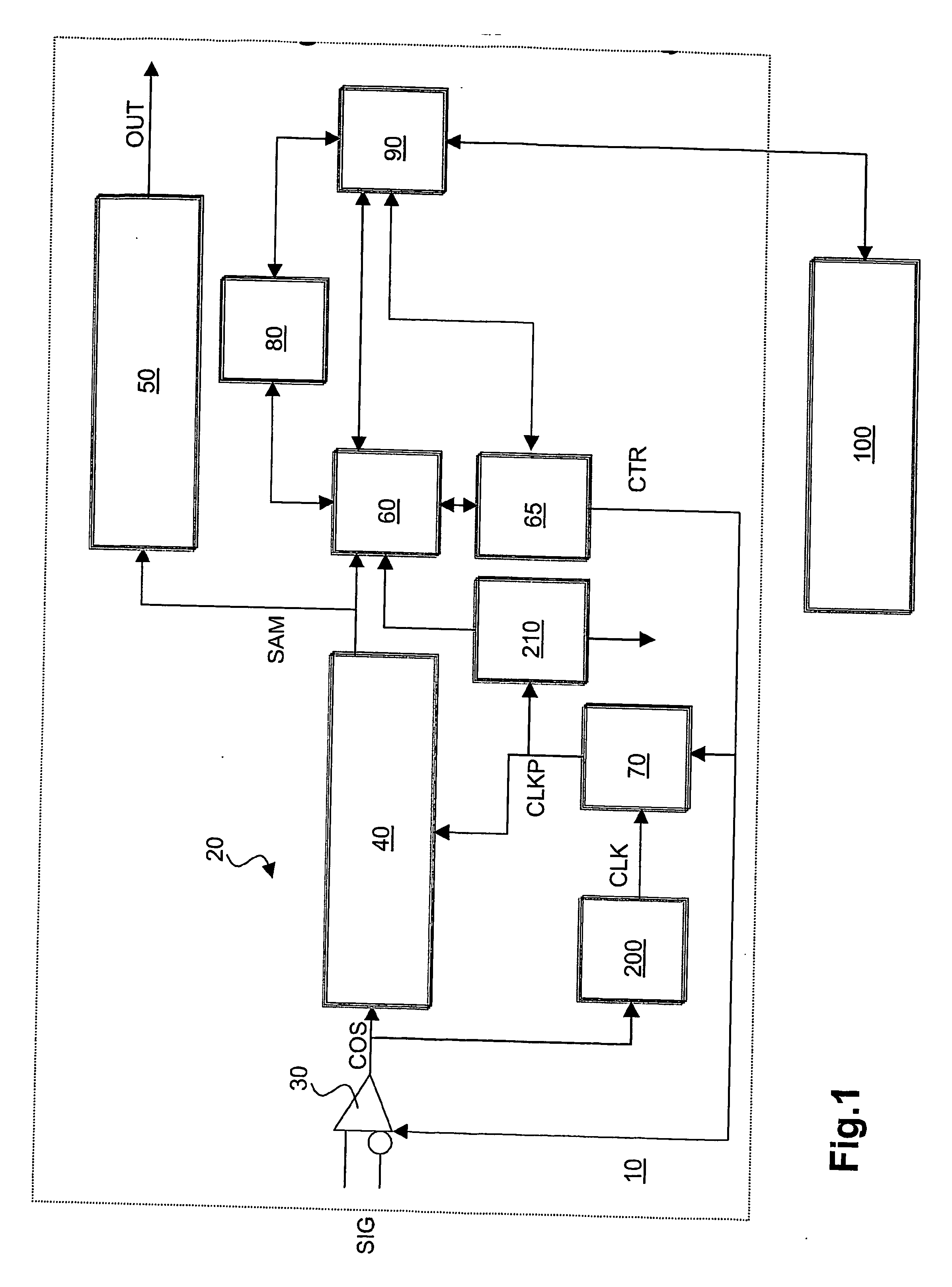
[0008]FIG. 1 shows an example of a preferred embodiment of an IC 10 according to the present invention. The IC 10 comprises an input unit 20 to receive an input signal SIG from external with respect of the IC 10. The input unit 20 comprises a level comparator 30 for comparing the input signal SIG and correspondingly providing a comparator output signal COS to a sampling unit 40 for sampling the comparator output signal COS.

[0009] The level comparator 30 can be any circuit allowing comparing levels of signals. In case of a single-ended input signal SIG, the level comparator 30 preferably compares the input signal SIG, or a signal derived therefrom, as comparator input signal against a threshold value. Such threshold can be e.g. a referenc


PUM


Abstract

An integrated circuit (10), preferably a field programmable gate array—FPGA or an application specific integrated circuit—ASIC—, comprises a level comparator (30) for comparing a level of a comparator input signal and correspondingly providing a comparator output signal (COS). A sampling unit (40) is coupled to the level comparator (30) for sampling (SAM) the comparator output signal (COS). A bit error test unit (60) receives the sampled comparator output signal (SAM) and determine therefrom an indication of a bit error in a sequence of the sampled comparator output signal (SAM).

Description


Claims


Application Information

Patent Timeline
Owner KEYSIGHT TECH
Why Eureka
Try Eureka