Voltage generation circuit and method thereof

a voltage generation circuit and voltage generation technology, applied in the direction of electric variable regulation, process and machine control, instruments, etc., can solve the problems of inability to stabilize the output voltage level in a shorter time, and the current characteristics of the mos transistor are more easily affected

Active Publication Date: 2007-12-27
SAMSUNG ELECTRONICS CO LTD
View PDF13 Cites 20 Cited by
  • Summary
  • Abstract
  • Description
  • Claims
  • Application Information

AI Technical Summary

Benefits of technology

The invention provides an improved way for generating small voltages that are stable over time or can be used up faster than usual by creating more efficient circuits.

Problems solved by technology

This patented technical problem addressed in this patent describes two types of circuits used during the process of producing stable voltages on integrated devices: one uses a single type of analog or digital signal generator (A/D) that generates both positive and negative signals based upon its own internal clock frequency; while the other relies solely on external sources like supply voltages. These issues can lead to unstable levels of electrical energy being supplied due to variations in manufacturing processes and temperatures affecting their performance.

Method used


Image

  • Voltage generation circuit and method thereof
  • Voltage generation circuit and method thereof
  • Voltage generation circuit and method thereof

Examples


Embodiment Construction

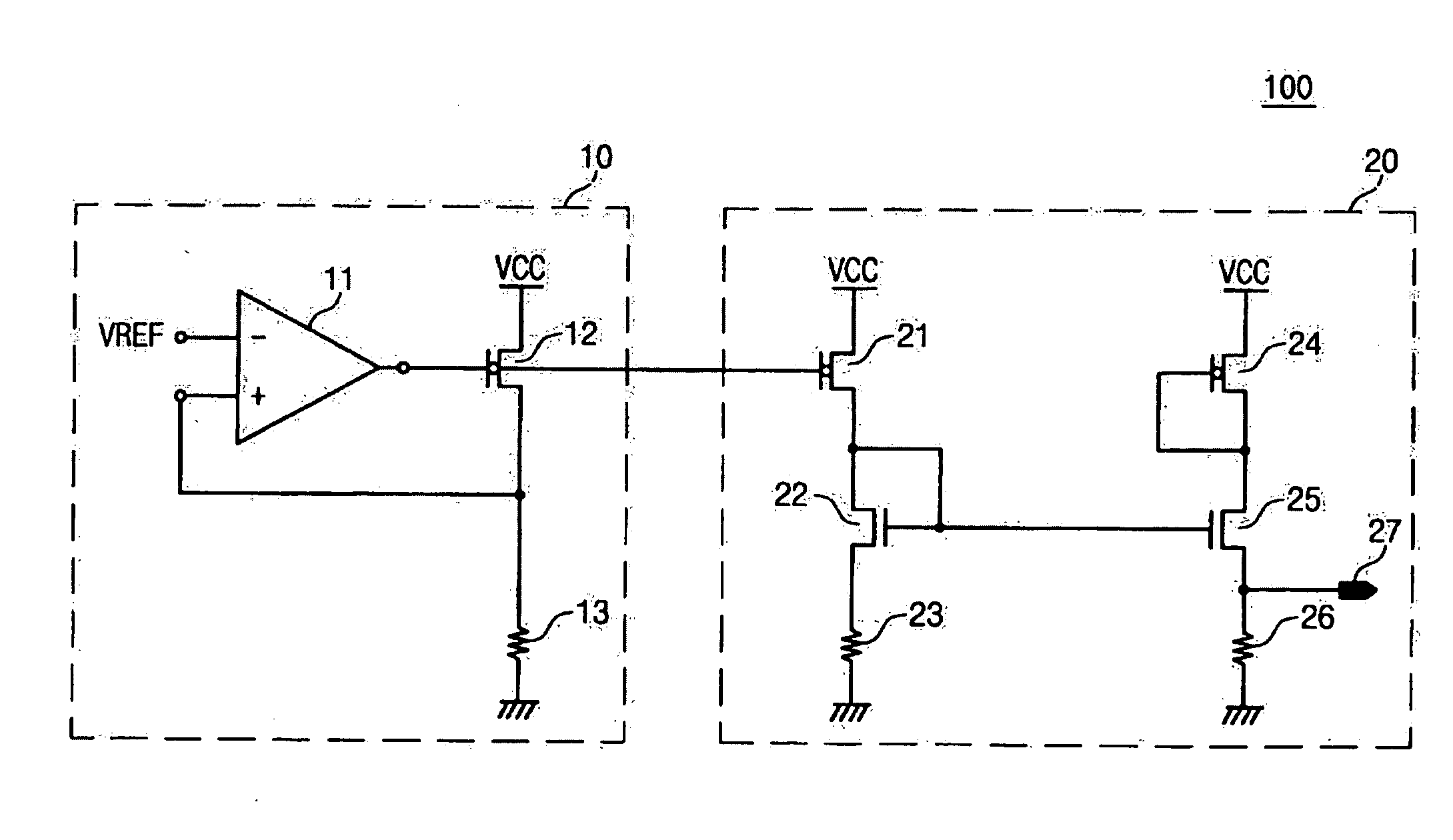
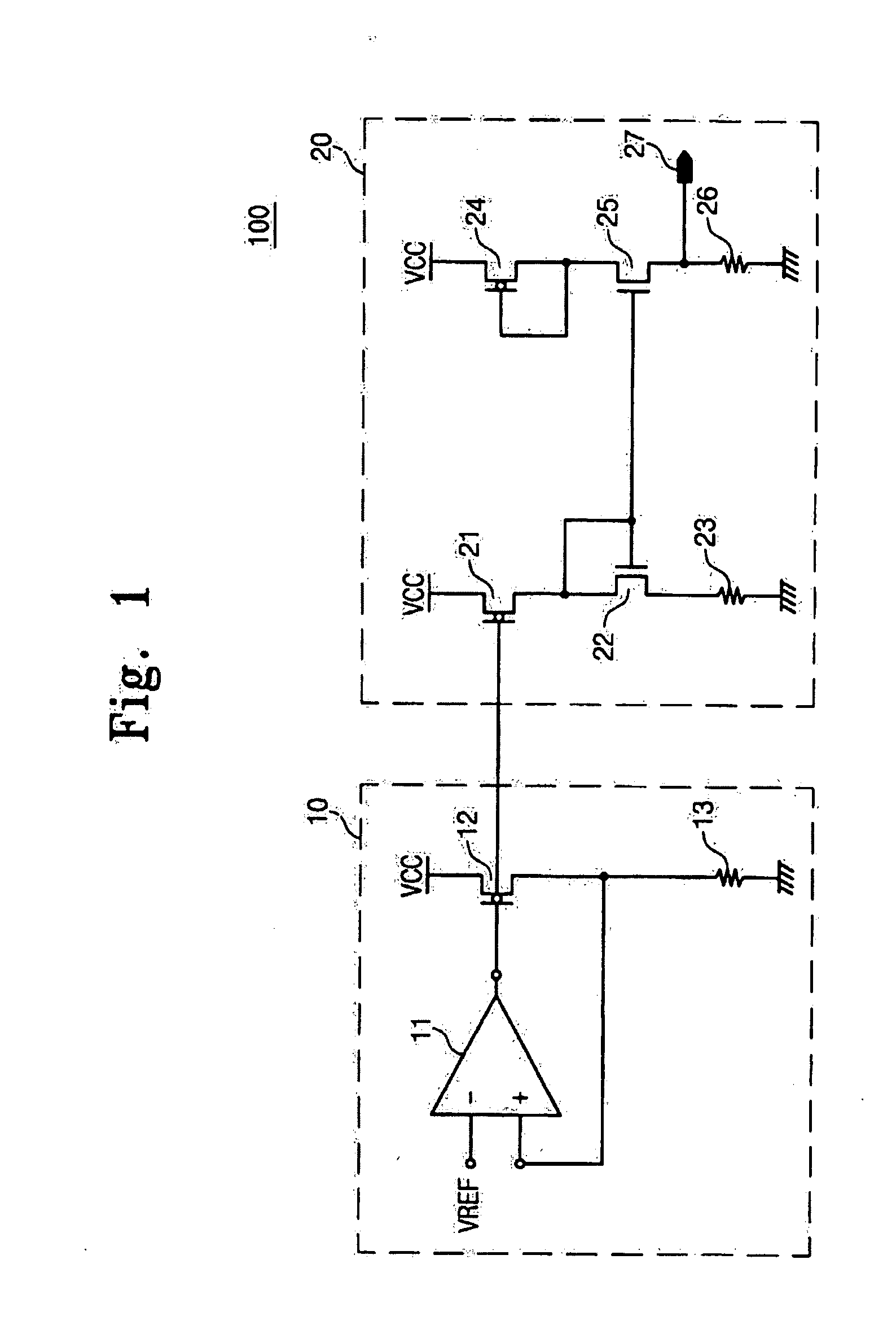
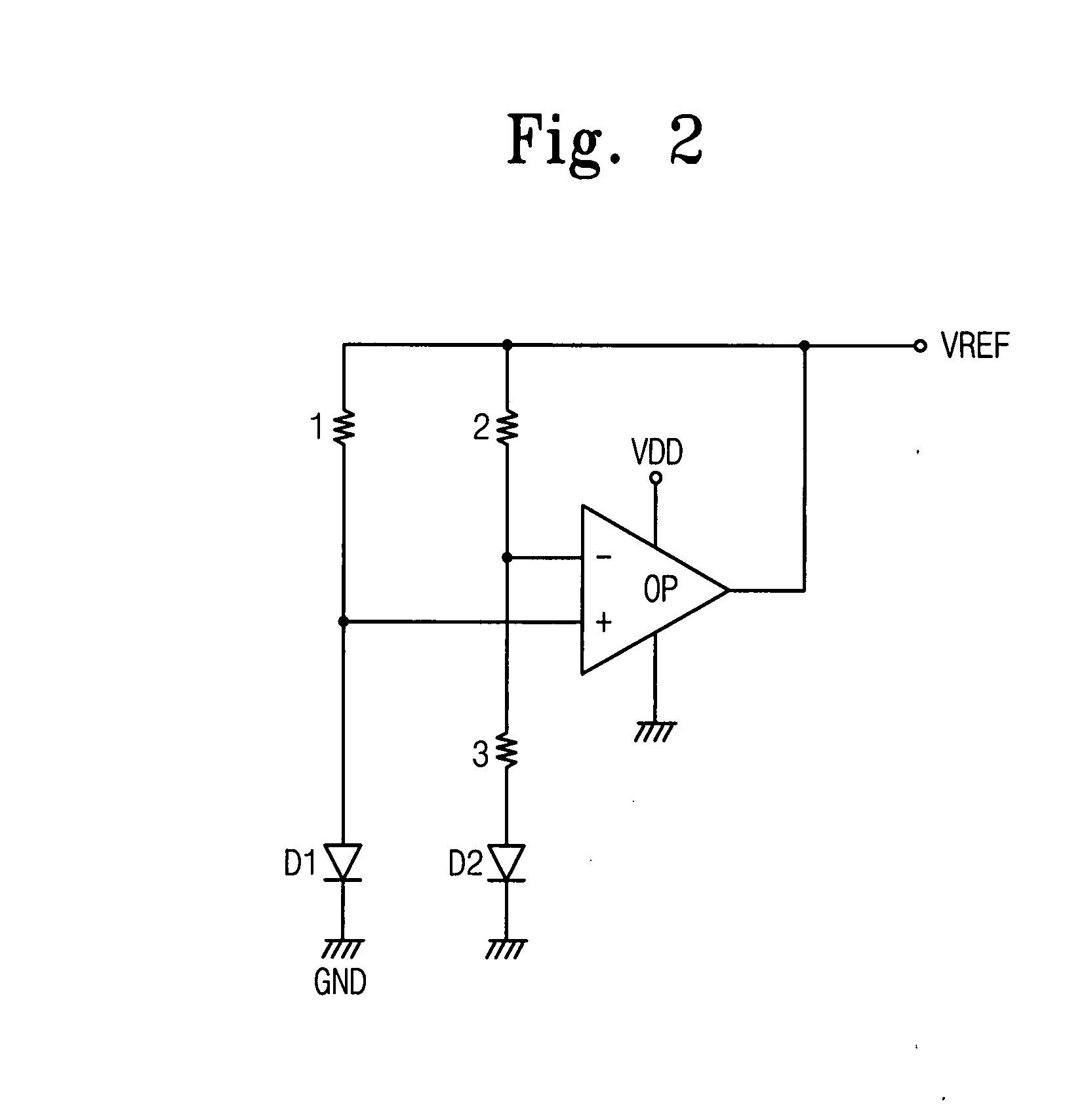
[0026]Example embodiments will now be described more fully hereinafter with reference to the accompanying drawings. Embodiments may, however, be in many different forms and should not be construed as being limited to the example embodiments set forth herein. Rather, these example embodiments are provided so that this disclosure will be thorough and complete, and will fully convey the scope to those skilled in the art. In the drawings, the thicknesses of layers and regions may be exaggerated for clarity.

[0027]It will be understood that when a component is referred to as being “on,”“connected to” or “coupled to” another component, it can be directly on, connected to or coupled to the other component or intervening components may be present. In contrast, when a component is referred to as being “directly on,”“directly connected to” or “directly coupled to” another component, there are no intervening components present. As used herein, the term “and / or” includes any and all combinations


PUM


Abstract

A voltage generation circuit may include a static current circuit and/or a current mirror. The static current circuit may include a first resistor. The current mirror may include a second resistor, a third resistor, and/or an output terminal.

Description


Claims


Application Information

Patent Timeline
Owner SAMSUNG ELECTRONICS CO LTD
Why Eureka
Try Eureka