Optical device and manufacturing method thereof

Active Publication Date: 2008-01-31
FUJITSU LTD
View PDF10 Cites 19 Cited by
  • Summary
  • Abstract
  • Description
  • Claims
  • Application Information

AI Technical Summary

Benefits of technology

[0046]According to the present invention, the second ferrule is fixed inside the support pipe, one end thereof is constructed to protrude toward the inner part of the package, and another end is constructed to substantially protrude at a tip part of the support pipe by a length required for the airtight fixing, and therefore when optical axis adjustments are made by connecting the optical fiber assembly in which the first ferrule is fixed to the optical fiber together with the second ferrule to the optical waveguide chip, the first ferrule and the second ferrule can be gripped directly and simultaneously inside the package. Consequently, the allowable bending radius of the optical fiber can reliably be secured even if the optical fiber is made shorter to reduce the size of optical waveguide device, and thus optical axis adjustment work itself can be simplified while achieving reduced device size and integration as an optical waveguide device, contributing to reduction in manufacturing costs as an optical waveguide device as well.
[0047]Also, according to the present invention, the second ferrule is fixed in

Problems solved by technology

With widespread use of the Internet, mobile phones, and advanced features of terminal equipment, increasing transmission capacity is a mandatory challenge.
Thus, communication networks are becoming increasingly dependent on optical fibers capable of high-speed, large-capacity transmission, and thus construction and maintenance of optical communication networks using WDM (Wavelength Division Multiplexing) is urgently needed.
However, since there is n

Method used


Image

  • Optical device and manufacturing method thereof
  • Optical device and manufacturing method thereof
  • Optical device and manufacturing method thereof

Examples


Example

[A] Description of the First Embodiment

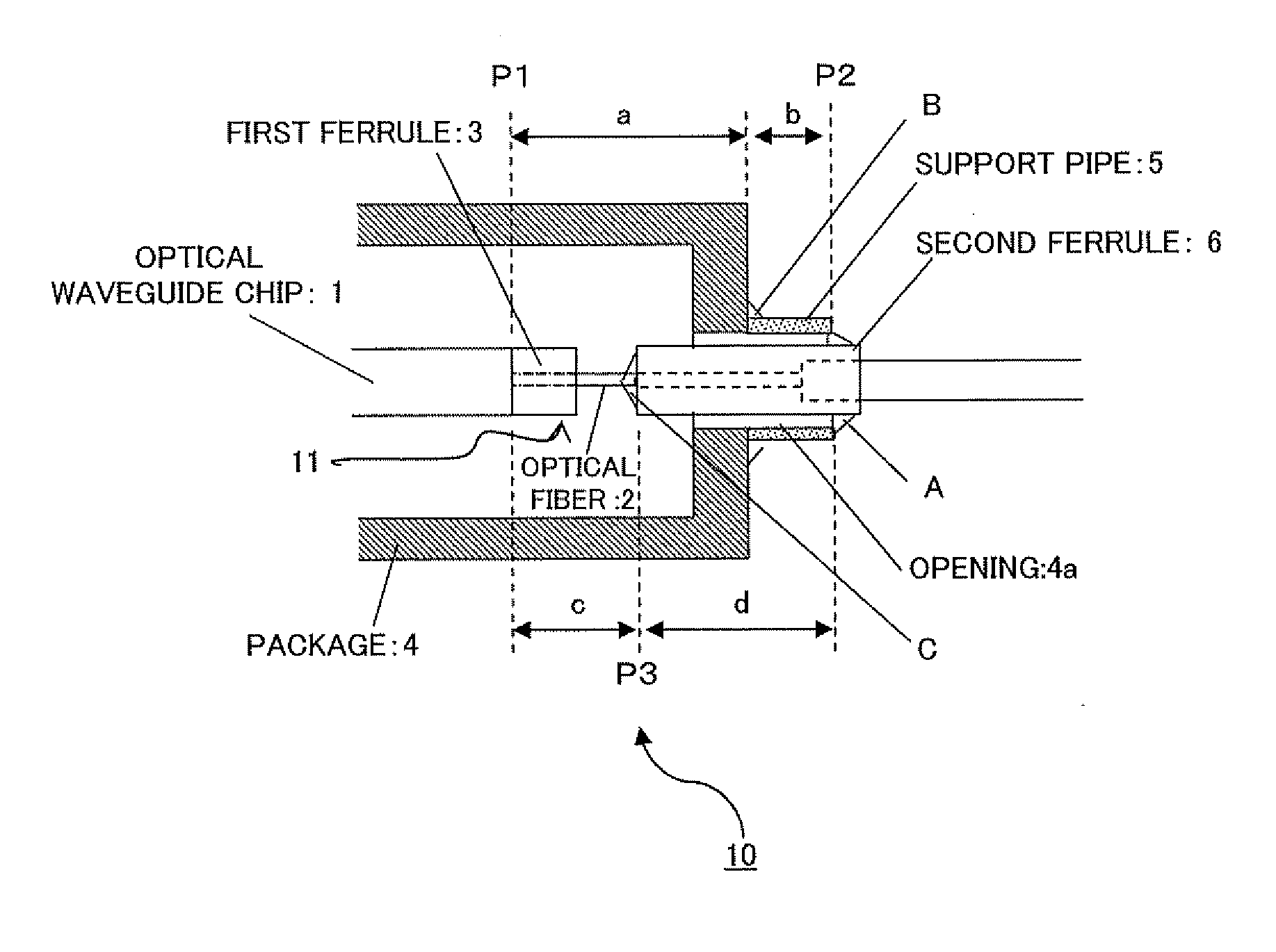
[0059]FIG. 1 is a schematic top view showing an optical waveguide device 10 according to the first embodiment of the present invention and shows the optical waveguide device 10 by focusing particularly on conduction connection of an optical waveguide chip 1 constituting the optical waveguide device 10 and an optical fiber 2 leading to the outside of a package 4. The optical waveguide device 10 shown in FIG. 1 comprises the optical waveguide chip 1, the optical fiber 2, a first ferrule 3, the package 4, a support pipe (first pipe) 5, and a second ferrule 6.

[0060]Here, the optical waveguide chip 1 is, for example, an LN substrate chip on which an optical waveguide is formed as an optical element and can be applied, for example, as a light modulation element chip (optical element chip) (See numeral 102 in FIG. 13) that performs light modulation of input light. The optical fiber 2 is optically connected to the optical waveguide constituting the optica

Example

[B] Description of the Second Embodiment

[0105]FIG. 4 is a schematic top view showing an optical waveguide device 20 according to the second embodiment of the present invention and shows the optical waveguide device 20 by focusing particularly on conduction connection of the optical waveguide chip 1 constituting the optical waveguide device 20 and the optical fiber 2 leading to the outside of the package 4. In contrast to the optical waveguide device 10 in the first embodiment described above, the optical waveguide device 20 shown in FIG. 4 has an enveloping pipe (second pipe) 12 mounted on the tip part of the second ferrule 6A on an inner side of the package 4. While the enveloping pipe 12 is mounted on a second ferrule 6A, other configuration is basically the same as that of the above-described first embodiment. The same numerals in FIG. 4 as those in FIG. 1 denote approximately the same components.

[0106]Here, the second ferrule 6A has the external diameter smaller than the internal d

Example

[C] Description of the Third Embodiment

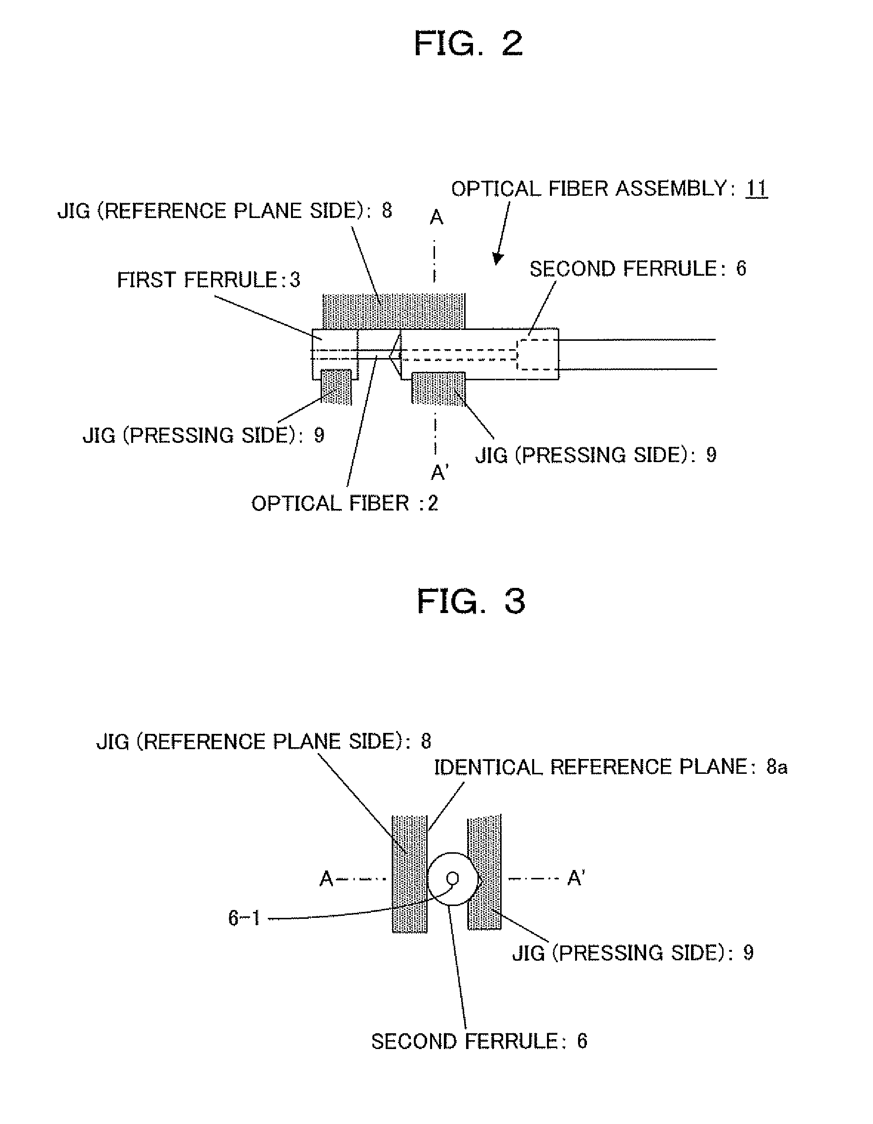
[0139]FIG. 7 is a schematic top view showing an optical waveguide device 30 according to the third embodiment of the present invention. The optical waveguide device 30 shown in FIG. 7 is different from the optical waveguide device 10 in the first embodiment described above in that 2-core optical fibers 2-1 and 2-2 are used for conduction. Accordingly, two fiber insertion holes are provided in first and second ferrules 35 and 6B respectively (See numerals 6-1 and 6-2 shown in FIG. 9 with respect to the second ferrule 6B). The same numerals in FIG. 7 as those in FIG. 1 denote approximately the same components.

[0140]When assembling the optical waveguide device 30 in the third embodiment, like the first embodiment (See numeral 11), an optical fiber assembly 31 shown in FIG. 8 is constructed from the first ferrule 3B, second ferrule 6B, and optical fibers 2-1 and 2-2. FIG. 9 shows an AA′ cross section shown in FIG. 8. As shown in FIG. 8 and FIG. 9, the


PUM


Abstract

The present invention is an optical device achieving miniaturization, functional integration, and cost reduction, and comprises an optical element chip, an optical fiber assembly comprised of an optical fiber, a first ferrule, and a second ferrule, a package containing and enveloping the optical element chip and having an opening for introducing the optical fiber assembly, and a support pipe mounted on an extension of the opening to support an introductory part of the optical fiber into the package together with the second ferrule constituting the optical fiber assembly to be introduced into the package and to hermetically seal the package, wherein the second ferrule is fixed inside the support pipe, one end thereof protrudes toward an inner part of the package, and another end substantially protrudes at a tip part of the support pipe by a length required for the airtight fixing.

Description


Claims


Application Information

Patent Timeline
Owner FUJITSU LTD
Why Eureka
Try Eureka