On-Chip Adaptive Voltage Compensation

a technology of voltage compensation and integrated circuit, applied in the field of system and method for regulating voltage to an integrated circuit, can solve the problems of increasing cost, reducing yield, and occupying more test time for integrated samples

Active Publication Date: 2008-08-07
IBM CORP
View PDF57 Cites 23 Cited by
  • Summary
  • Abstract
  • Description
  • Claims
  • Application Information

AI Technical Summary

Benefits of technology

The present invention provides an improved way to measure the voltage supplied by a voltage regulator (VR) circuit for controlling its voltage. This helps improve the performance of electronic devices that use this technology.

Problems solved by technology

The technical problem addressed by this patent is how to improve the quality control (QC) of integrated circuits during production while ensuring consistently high yields from failures caused by poor performance testing. Current methods involve testing each sample individually before shipping them separately, but this can result in reduced productivity and increased costs associated with maintaining strict specifications.

Method used


Image

  • On-Chip Adaptive Voltage Compensation
  • On-Chip Adaptive Voltage Compensation
  • On-Chip Adaptive Voltage Compensation

Examples


Embodiment Construction

[0017]The following is intended to provide a detailed description of an example of the invention and should not be taken to be limiting of the invention itself. Rather, any number of variations may fall within the scope of the invention, which is defined in the claims following the description.

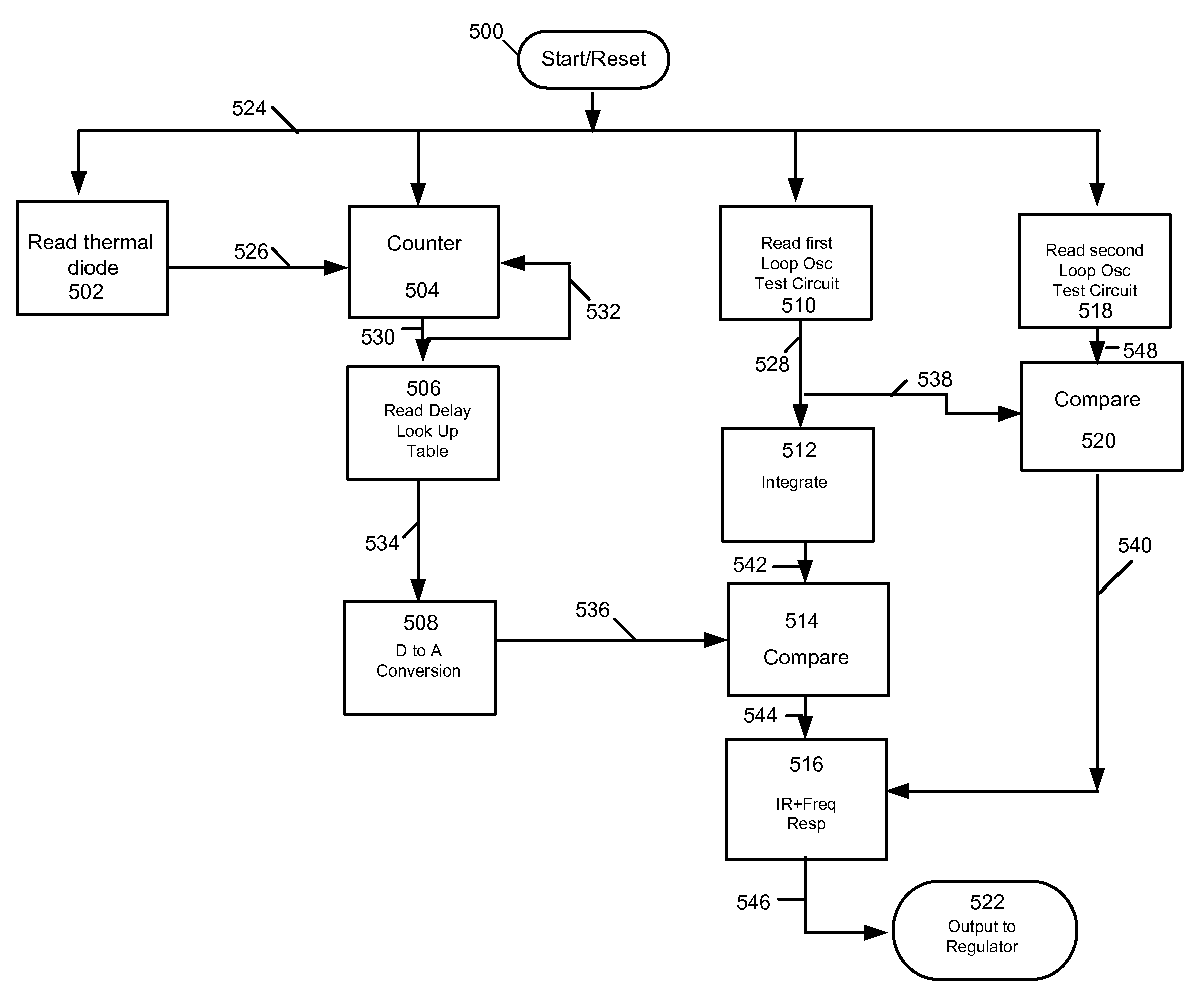
[0018]The present invention provides a system to measure operating conditions on an integrated circuit and adjust voltage (Vdd) provided to the integrated circuit to either increase performance of the integrated circuit or save power expended by the integrated circuit.

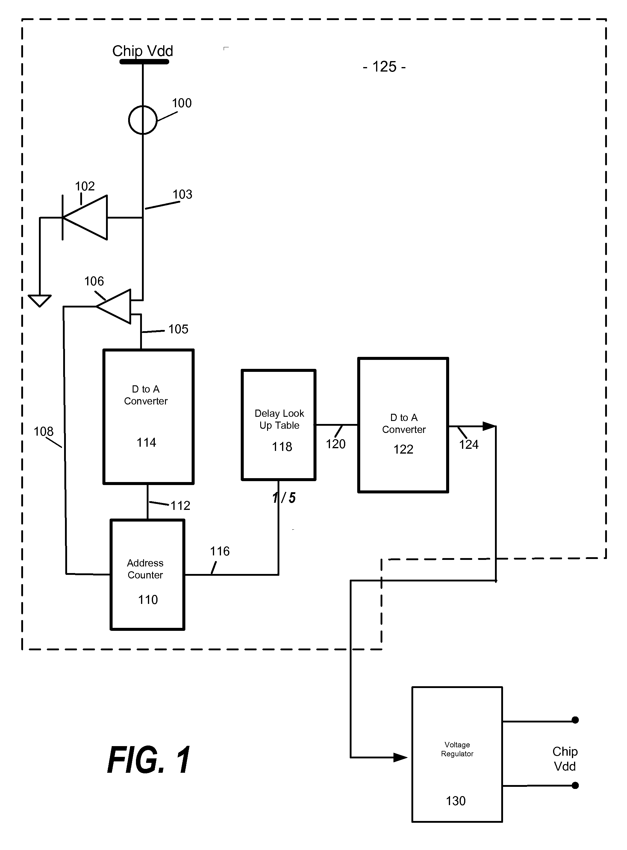
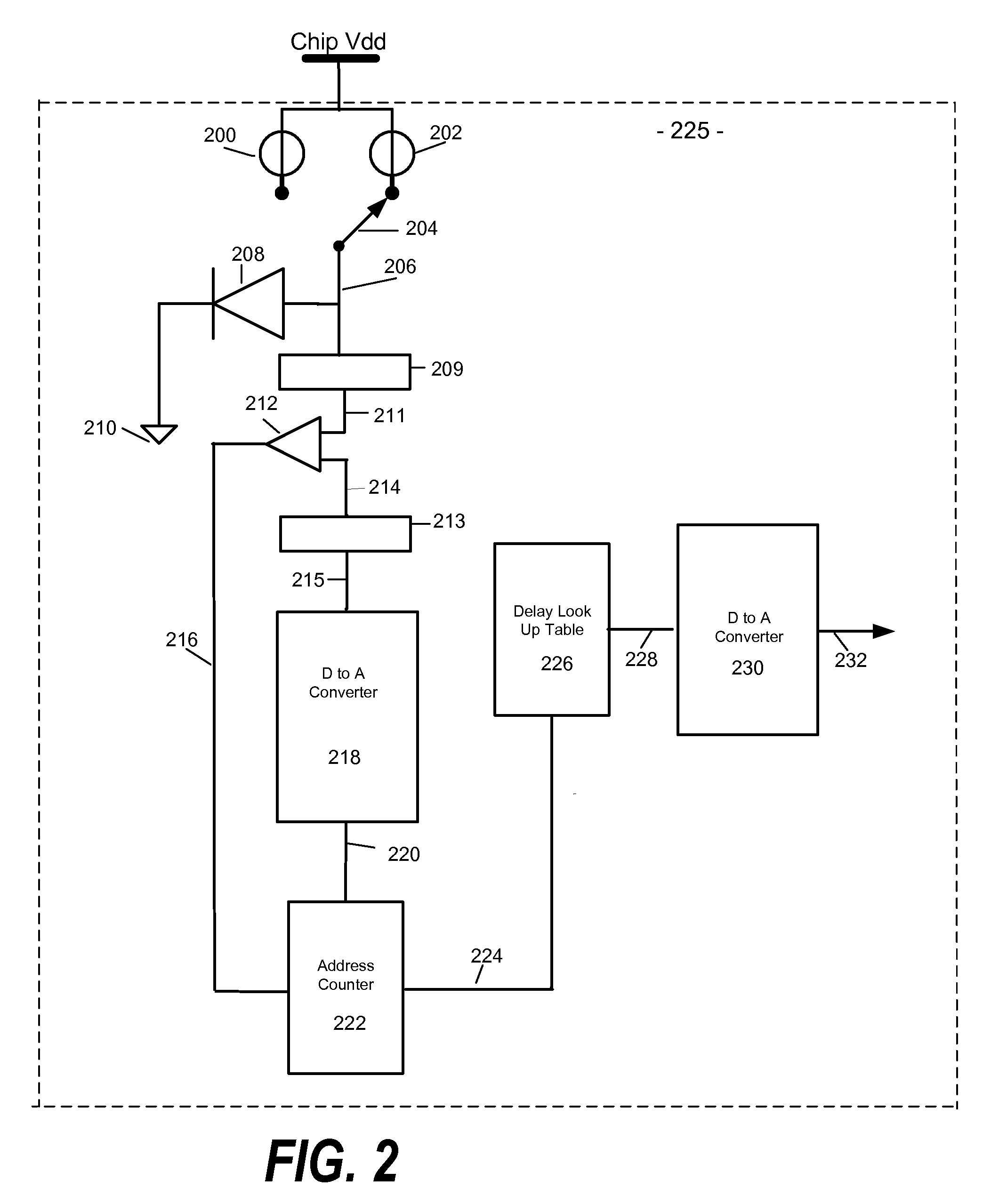
[0019]In the preferred embodiment, three physical condition measurements are made. The first is temperature, which is measured by a thermal diode on the surface of the integrated circuit. The second is the IR (voltage) drop measured by two ring oscillator circuits and the third is the frequency performance of the integrated circuit measured by a single loop oscillator compared to stored predetermined performance values.

[0020]The com


PUM


Abstract

Measurement circuit components are included in an integrated circuit fabricated on a semiconductor substrate. These measurement circuits are connected to a voltage regulation circuit that provides the integrated circuit voltage source. These measurement circuits provide signals to control the voltage regulation circuit to adjust the voltage output to the integrated circuit based upon a measurement values obtained on the semiconductor device. These measurements include temperature and IR drop at locations on the semiconductor substrate, along with the frequency response of integrated circuit.

Description


Claims


Application Information

Patent Timeline
Owner IBM CORP
Why Eureka
Try Eureka