Bias Current Generator
a current generator and bias technology, applied in pulse generators, pulse techniques, instruments, etc., can solve the problems of requiring a lot of chip area for resistors with such high resistance, affecting the power supply of the generator, and limiting the range and flexibility of vsub>be /sub>be, etc., to achieve less chip area and less power consumption.
- Summary
- Abstract
- Description
- Claims
- Application Information
AI Technical Summary
Benefits of technology
Problems solved by technology
Method used
Image

Examples
Embodiment Construction
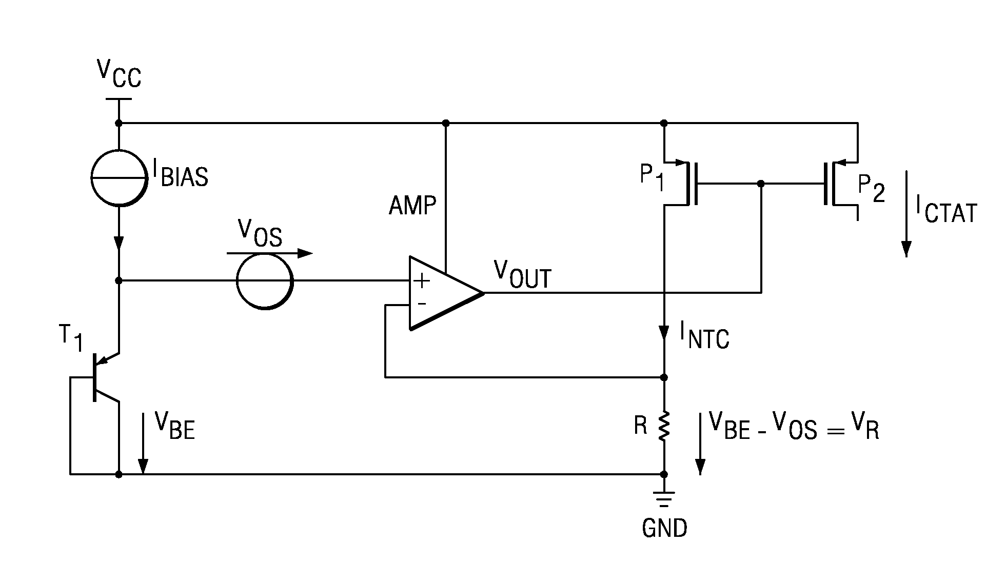
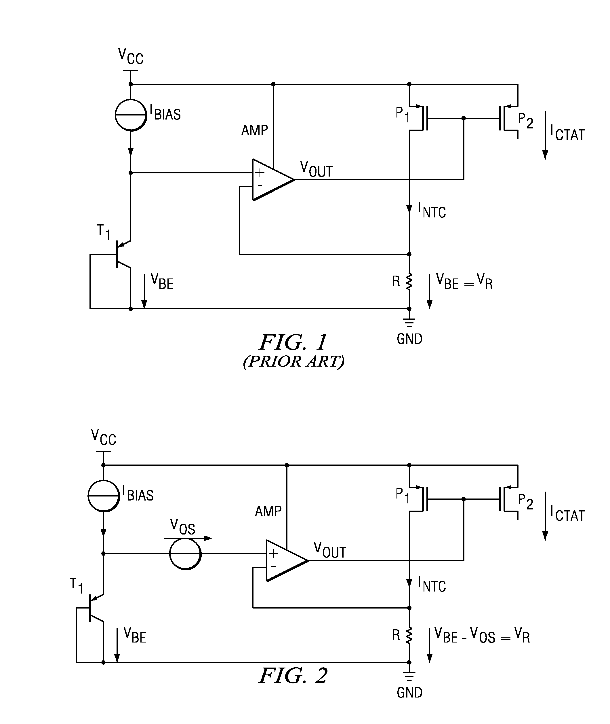
[0013]FIG. 1 shows a simplified block diagram of an NTC current generator according to the prior art. Bipolar transistor T1 has a base to emitter voltage VBE. The transistor receives a bias current Ibias from a constant current source. The base to emitter voltage VBE is coupled to the positive input of a differential amplifier AMP. The output of the amplifier AMP is coupled to the gates of PMOS transistors P1 and P2. The source of PMOS transistor P1 is coupled to a supply voltage VCC and its drain is coupled to the negative input of the amplifier AMP and a resistor R. Due to the feedback connection of the amplifier AMP, the base to emitter voltage VBE of bipolar transistor T1 also appears across resistor R. The output current ICTAT at PMOS transistor P2 is used for further biasing purposes having the desired temperature coefficient (TC). The TC of the output current ICTAT can be negative. However, the NTC can also be partially compensated or completely compensated by a PTC of the resis
PUM
 Abstract
Description
Claims
Application Information
 - R&D Engineer
- R&D Manager
- IP Professional
- Industry Leading Data Capabilities
- Powerful AI technology
- Patent DNA Extraction
Browse by: Latest US Patents, China's latest patents, Technical Efficacy Thesaurus, Application Domain, Technology Topic.
© 2024 PatSnap. All rights reserved.Legal|Privacy policy|Modern Slavery Act Transparency Statement|Sitemap