Agc circuit

Active Publication Date: 2009-04-16
GK BRIDGE 1
View PDF3 Cites 17 Cited by
  • Summary
  • Abstract
  • Description
  • Claims
  • Application Information

AI Technical Summary

Benefits of technology

[0048]According to the present invention, it is possible to provide the AGC circuit that can also be incorporated in an integrated circuit easily without the needs of the integrating circ

Problems solved by technology

Meanwhile, if a DC offset voltage is included in the input signal of the AGC circuit, the DC offset voltage affects an AGC operation adversely, and thus the AGC operation is not performed normally.
Additionally, particularly in the aud

Method used


Image

  • Agc circuit
  • Agc circuit
  • Agc circuit

Examples


first embodiment

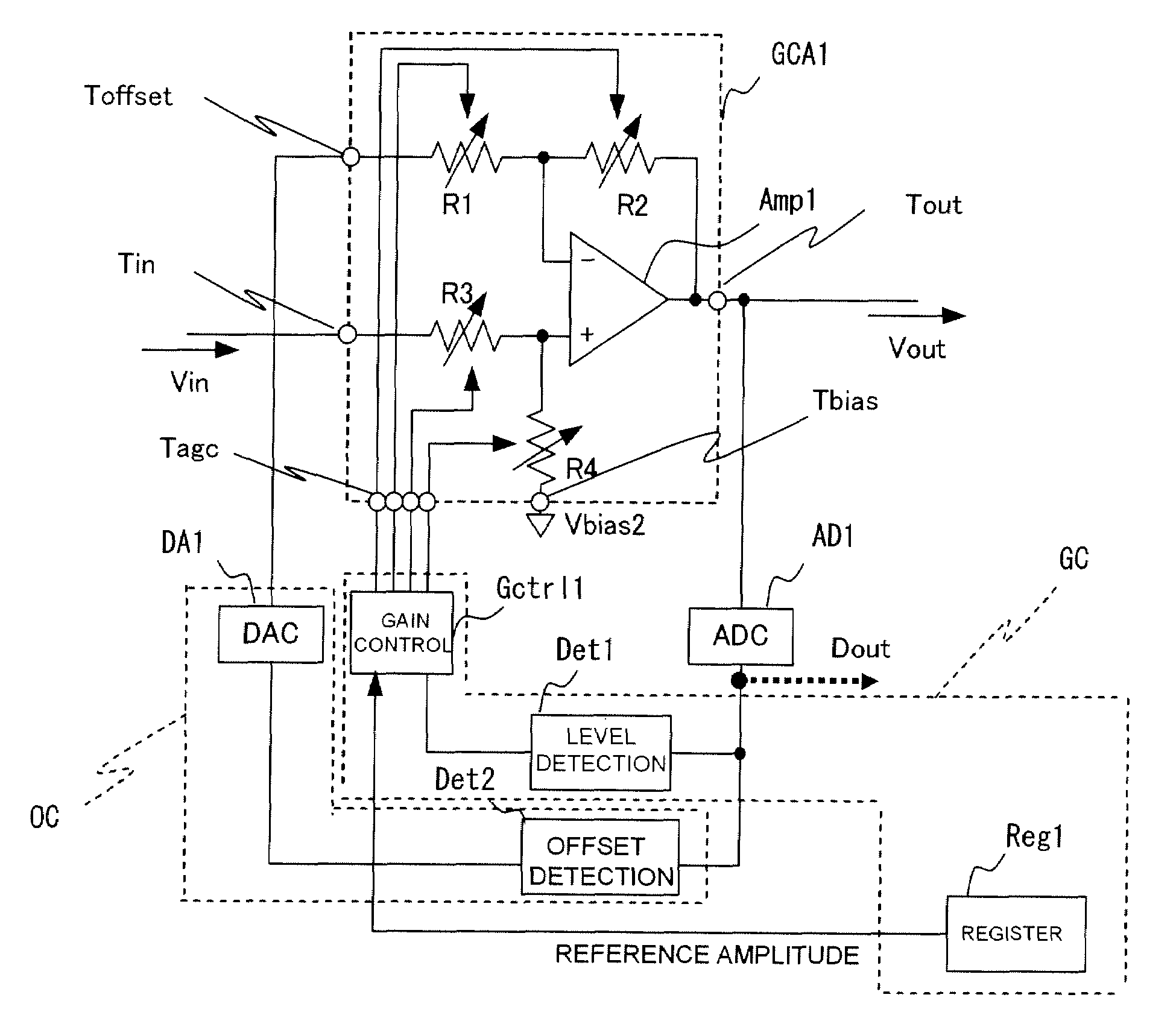
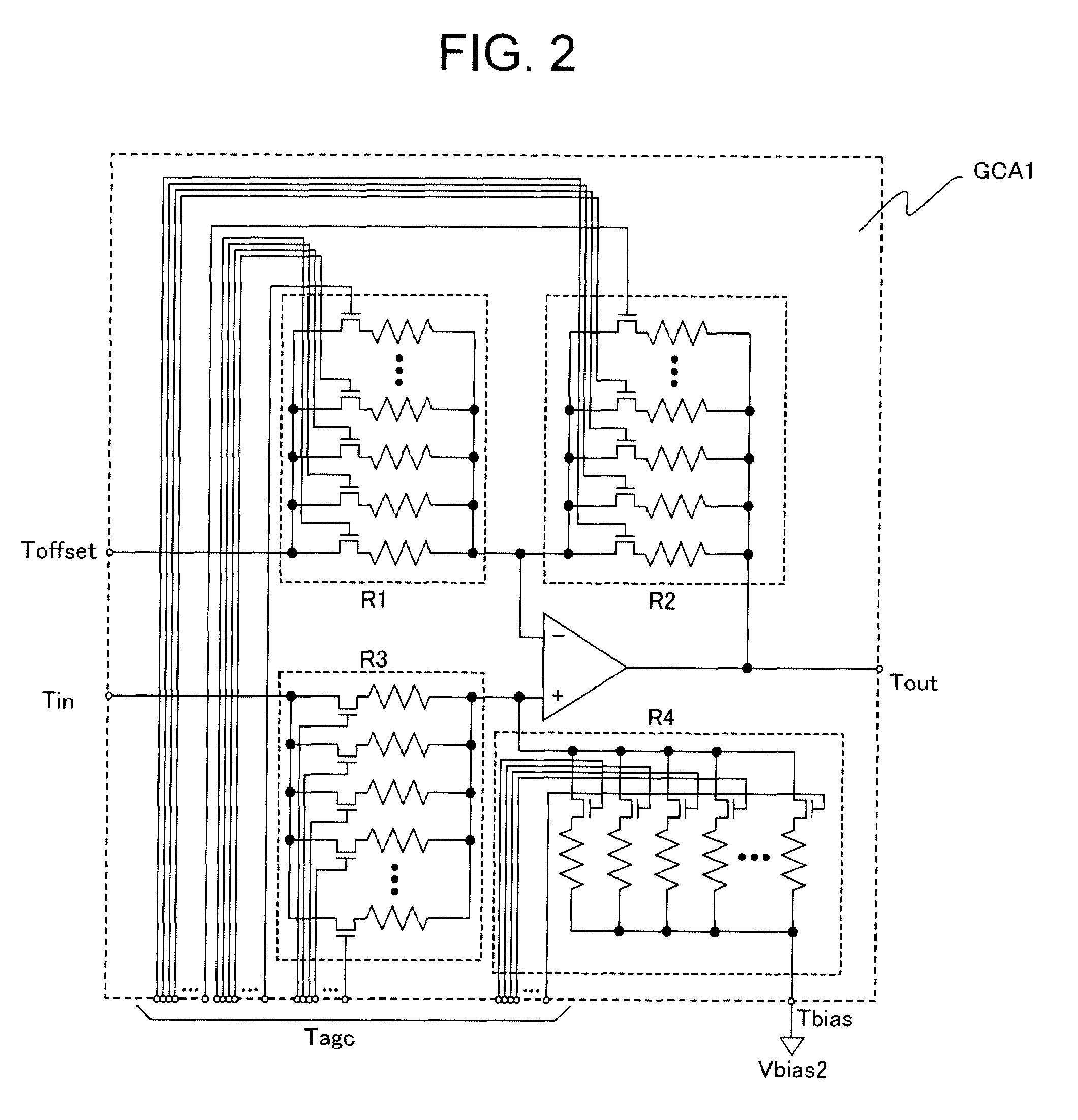
[0080]FIG. 1 shows a typical configuration of an AGC circuit in accordance with a first embodiment of the present invention.

[0081]In FIG. 1, symbol GCA1 represents a variable gain amplifying circuit constituted by a differential amplifying circuit Amp1, and variable resistors R1, R2, R3, and R4. Symbol Tin represents a signal input terminal into which an analog voltage, for example, an analog audio signal or the like, is inputted. Symbol Tout represents a signal output terminal from which an amplified or attenuated analog voltage is outputted, for example. Symbol Tagc represents gain control terminals into which gain control signals are inputted. Symbol Toffset represents an offset compensation terminal into which an offset compensation signal is inputted. Symbol Tbias represents a reference voltage terminal into which a reference voltage for determining an output bias voltage is inputted.

[0082]Symbol AD1 represents an A / D conversion circuit for A / D converting an output signal of t

second embodiment

[0136]FIG. 12 shows a configuration of an AGC circuit in accordance with a second embodiment of the present invention.

[0137]In FIG. 12, description will be omitted by giving the same symbol to the same component as that of the AGC circuit shown in FIG. 9, and only components which are newly added to the AGC circuit shown in FIG. 1 will be described.

[0138]In FIG. 12, n (n≧2) variable gain amplifying circuits GCA1, GCA2, . . . , GCAn, n gain control signal holding circuits GLatch1, GLatch2, . . . , GLatchn, n offset compensation signal holding circuits OLatch1, OLatch2, . . . , OLatchn, a selector circuit MUX1 that receives output signals Vout1, Vout2, . . . , Voutn of the variable gain amplifying circuits GCA1, GCA2, . . . , GCAn, and selects one of them to then output it to an A / D converter AD1, and a mode control circuit Ctrl3 that controls a signal selection, a gain control operation, and the offset compensation operation are arranged in this AGC circuit.

[0139]Signals Vin1, Vin2, .


PUM


Abstract

There is provided an AGC circuit that has a very small offset voltage and is easy for integration, without using any of external capacities. For that reason, a variable gain amplifying circuit (GCA1) which has a gain controlled by a gain control signal, and whose output DC offset is controlled by an offset compensation signal, an A/D conversion circuit (AD1) for A/D converting an output signal of this variable gain amplifying circuit (GCA1), a level detection circuit (Det1) for performing peak detection of an output signal of this A/D conversion circuit (AD1) to thereby detect an amplitude level, a gain control circuit (Gctrl1) for outputting a gain control signal according to an output signal of this level detection circuit (Det1), an offset detection circuit (Det2) provided with a lowpass filter for taking out a DC component from the output signal of the A/D conversion circuit (AD1), and a D/A conversion circuit (DA1) for D/A converting an output signal of the offset detection circuit (Det2) to thereby output the offset compensation signal are provided.

Description


Claims


Application Information

Patent Timeline
Owner GK BRIDGE 1
Why Eureka
Try Eureka