Buffer circuit of semiconductor memory apparatus
a buffer circuit and memory device technology, applied in the direction of logic circuit coupling/interface arrangement, pulse generator, pulse technique, etc., can solve problems such as reference voltage noise, and achieve the effect of decreasing reducing or increasing the voltage level of output nodes
- Summary
- Abstract
- Description
- Claims
- Application Information
AI Technical Summary
Benefits of technology
Problems solved by technology
Method used
Image

Examples
Embodiment Construction
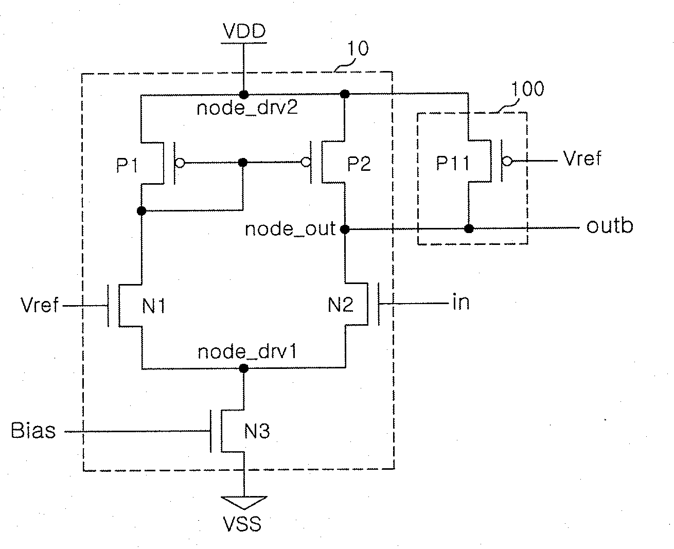
[0017]A buffer circuit of a semiconductor memory apparatus according to one embodiment can be configured to include a buffering section 10 and a voltage compensation section 100 as shown in FIG. 2.
[0018]The buffering section 10 can decrease or increase a voltage level of an output node node_out to determine a level of an output signal ‘outb’ by comparing a voltage level of an input signal ‘in’ with a reference voltage ‘Vref’. For example, the buffering section 10 can output the output signal ‘outb’ of a low level when the voltage level of the input signal ‘in’ is higher than the reference voltage ‘Vref’. Meanwhile, the buffering section 10 can output the output signal ‘outb’ of a high level when the voltage level of the input signal ‘in’ is lower than the level of the reference voltage ‘Vref’. At this time, the reference voltage ‘Vref’ is generated to detect the voltage level of the input signal ‘in’ and the voltage level of the reference voltage ‘Vref’ is generated at a target level w
PUM
 Abstract
Description
Claims
Application Information
 - R&D Engineer
- R&D Manager
- IP Professional
- Industry Leading Data Capabilities
- Powerful AI technology
- Patent DNA Extraction
Browse by: Latest US Patents, China's latest patents, Technical Efficacy Thesaurus, Application Domain, Technology Topic.
© 2024 PatSnap. All rights reserved.Legal|Privacy policy|Modern Slavery Act Transparency Statement|Sitemap