Data processing system with protocol determination circuitry

Active Publication Date: 2015-02-05
NXP USA INC
View PDF12 Cites 8 Cited by
  • Summary
  • Abstract
  • Description
  • Claims
  • Application Information

AI Technical Summary

Problems solved by technology

However, at the time of design, it is unknown what type of PMIC might be used to interface with the IC.

Method used


Image

  • Data processing system with protocol determination circuitry
  • Data processing system with protocol determination circuitry
  • Data processing system with protocol determination circuitry

Examples


Embodiment Construction

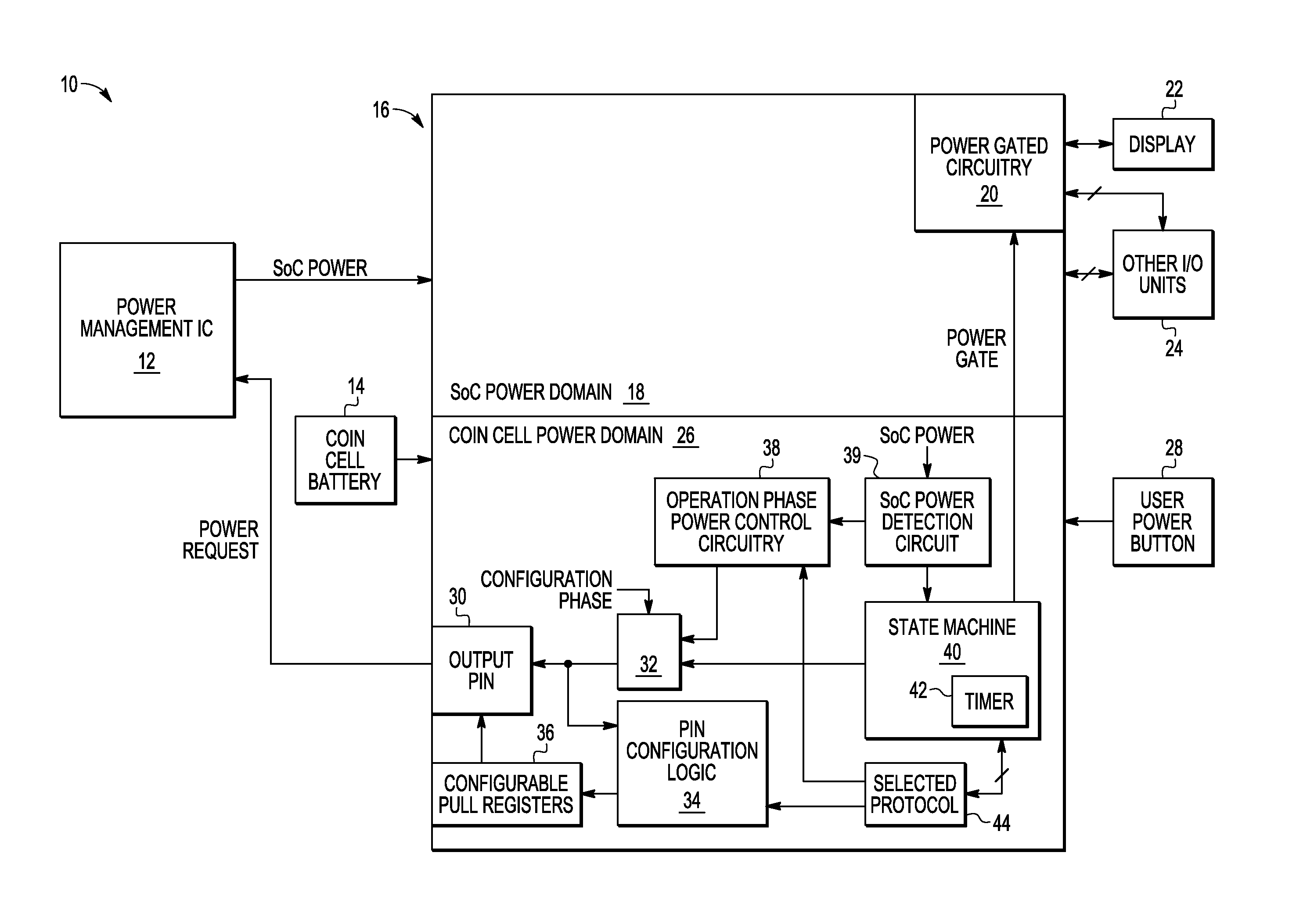
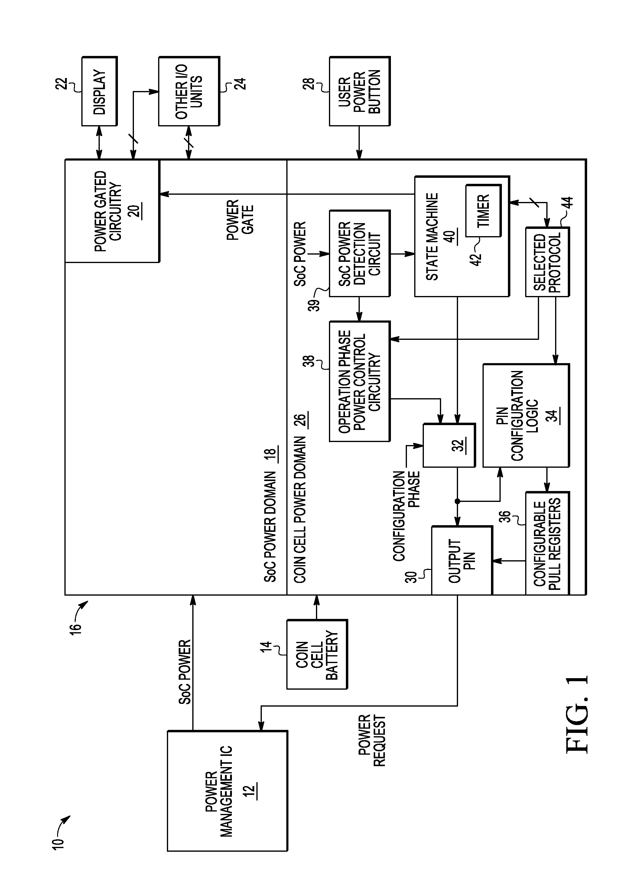
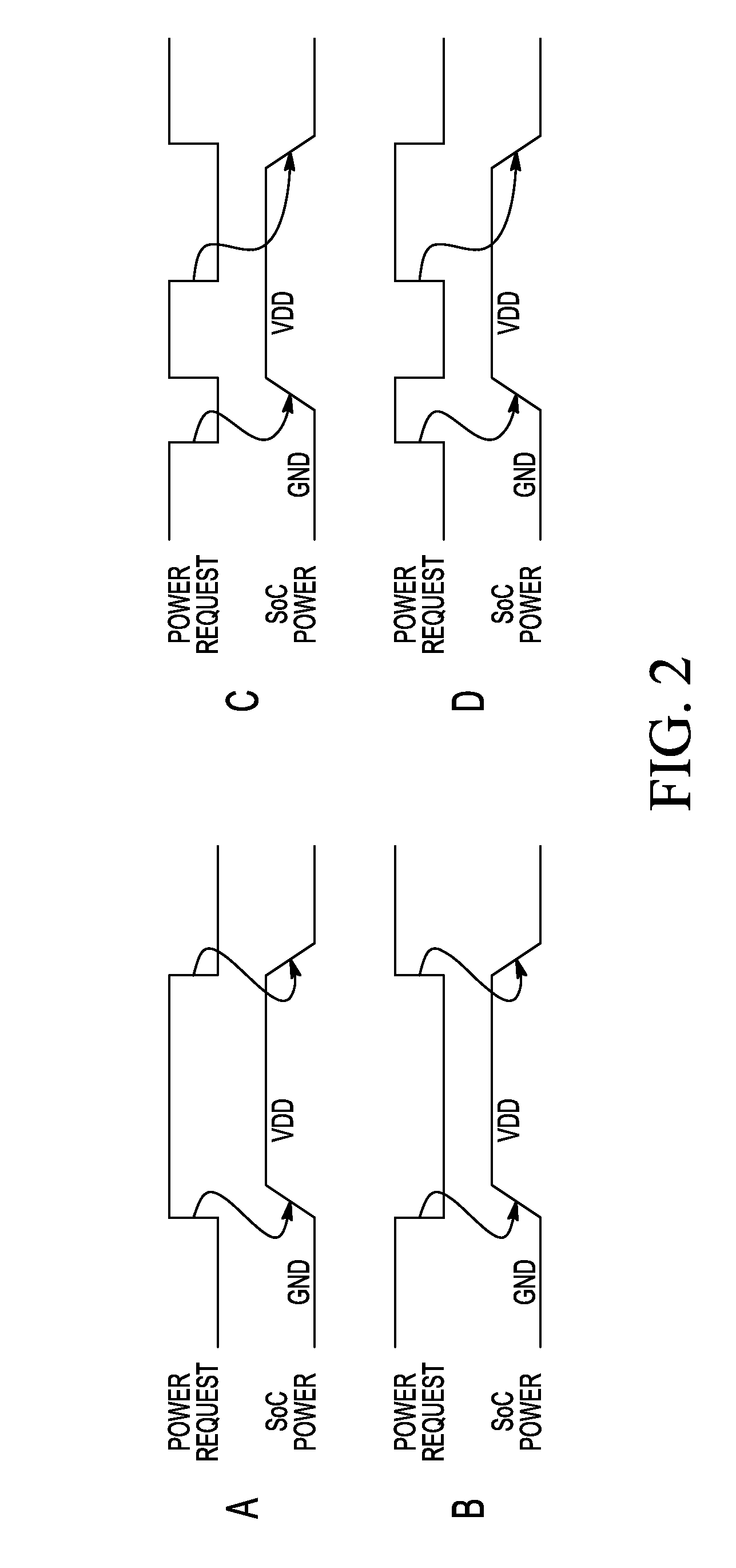
[0022]In one embodiment, an IC includes circuitry which is powered by a PMIC and circuitry which is powered by a low power source, such as a coin cell battery. The circuitry powered by the PMIC is located within an SoC power domain. The SoC may include any number and type of circuits which receive power provided by the PMIC. The circuitry powered by the low power source is located within a lower power domain, which may be referred to as a coin cell power domain. Upon initially applying power to the coin cell power domain, the circuitry within this domain determines the protocol of the PMIC. During this configuration phase, circuitry within the coin cell power domain provides test signals by way of an output pin to the PMIC and monitors the power provided by the PMIC to the IC in response to these test signals in order to determine the protocol of the PMIC. Determining the protocol of the PMIC includes determining whether the PMIC provides power in response to a toggle-mode signal or to


PUM


Abstract

A semiconductor device includes a processing system including a section of power domain circuitry and a section of coin cell power domain circuitry. The coin cell power domain circuitry is configured to, when power is initially provided to the coin cell power domain circuitry, using power provided by a power management circuit as feedback to determine that the power management circuit provides the power in response to a power request signal being a toggle signal, and determine that the power management circuit provides the power in response to the power request signal being a pulse signal.

Description


Claims


Application Information

Patent Timeline
Owner NXP USA INC
Why Eureka
Try Eureka