TTL and CMOS compatible input buffer

An input buffer and compatible technology, applied in the direction of logic circuit connection/interface layout, logic circuit coupling/interface using field effect transistors, etc., can solve problems such as flip point changes, achieve large gain margins, save costs, Effect of Improving Open-Loop Frequency Response

Active Publication Date: 2008-10-08
BEIJING MXTRONICS CORP +1
View PDF0 Cites 11 Cited by
  • Summary
  • Abstract
  • Description
  • Claims
  • Application Information

AI Technical Summary

Benefits of technology

This patented technology allows for better performance at both operating points while reducing costs associated with fabricating an integrated device (IC). It uses a specific type of transistor called CMos instead of traditional MOSFETs used in electronic devices such as logic gates or memory chips. By setting this value differently from previous designs, it becomes possible to achieve greater efficiency without increasing their size beyond what was previously necessary due to factors like temperature variations affecting its operation. Additionally, there're also included a frequency compensated network system to improve the opening loop frequency response over time. Overall, these technical improvements make IC design more efficient and effective than current methods.

Problems solved by technology

This technical problem addressed in this patents relates to improving the performance (power consumption reduction) of bimodal integrated circuits used in analog/digital systems such as digital communication receivers or transmitters due to their high impedance characteristics compared to other components like resistors. To address these issues, certain techniques were developed including reducing the number of pins needed on both the chip's ILD layer and connecting them closer together near one half of what allows for better noise immunity without adding extra wires. Additionally, the use of specific voltages for different parts within the circuit also helps maintain stability during dynamic operations while minimizing power dissipation.

Method used


Image

  • TTL and CMOS compatible input buffer
  • TTL and CMOS compatible input buffer
  • TTL and CMOS compatible input buffer

Examples


Embodiment Construction

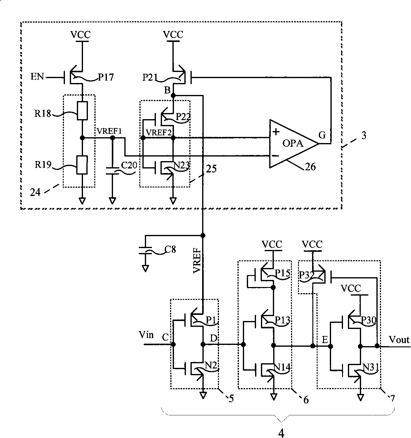
[0025] like figure 1 Shown is the schematic block diagram of the circuit of the TTL and CMOS compatible input buffer of the present invention, including a reference voltage generator 3 and an input buffer 4, and the reference voltage generator 3 includes a resistor divider network 24, a reference input buffer 25 and an operation The amplifier 26 and the input buffer 4 include an input inverter 5 , a second-stage input inverter 6 and a third-stage input inverter 7 .

[0026] The MOS transistors used in the present invention are all enhanced devices.

[0027] The input inverter 5 in the input buffer 4 is composed of a PMOS transistor P1 and an NMOS transistor N2, and the gate of the PMOS transistor P1 is connected to the gate of the NMOS transistor N2 as the input terminal of the input inverter 5, and the gate of the PMOS transistor P1 The drain is connected to the drain of the NMOS transistor N2 as the output terminal of the input inverter 5 , the source of the NMOS transistor N2


PUM


Abstract

A TTL and CMOS compatible type input buffer comprises a reference voltage generator and an input buffer which comprises at least one stage input invertor which include a PMOS tube P1 and an NMOS tube N2, the grids of which are connected as an input end for inputting signal Vin, a source pole of the PMOS tube P1 is connected with a reference voltage VREF provided by the reference voltage generator; when the circuit works in the TTL mode, the reference voltage generator provides reference voltage VREF for the input invertor between 3.3 and 3.5 V, the turning point voltage of the input invertor is 1.4 V to make input noise margin maximum; when the circuit works in the CMOS mode, the reference voltage generator has no quiescent power dissipation, the reference voltage generator provides reference voltage VREF for the input invertor between 4.6 and 5 V, the turning point voltage of the input invertor is 2.5 V to obtain the maximum noise margin.

Description


Claims


Application Information

Patent Timeline
Owner BEIJING MXTRONICS CORP
Why Eureka
Try Eureka