Method for separating sapphire substrate by unit on basis of stress action

A technology of sapphire substrate and stress action, which is applied in the direction of electrical components, semiconductor/solid-state device manufacturing, circuits, etc., can solve the problem of low yield rate of laser stripping, achieve the effect of ensuring unit independence and improving yield rate

Active Publication Date: 2011-04-06
FUJIAN JING AN OPTOELECTRONICS CO LTD
View PDF2 Cites 2 Cited by
  • Summary
  • Abstract
  • Description
  • Claims
  • Application Information

AI Technical Summary

Problems solved by technology

[0005] In order to solve the above-mentioned problem of low laser lift-off yield, the present invention innovativ

Method used


Image

  • Method for separating sapphire substrate by unit on basis of stress action
  • Method for separating sapphire substrate by unit on basis of stress action
  • Method for separating sapphire substrate by unit on basis of stress action

Examples


Embodiment Construction

[0023] The present invention will be further described below in conjunction with the accompanying drawings and embodiments.

[0024] A method for separating a sapphire substrate unit by unit based on stress, the preparation steps are as follows:

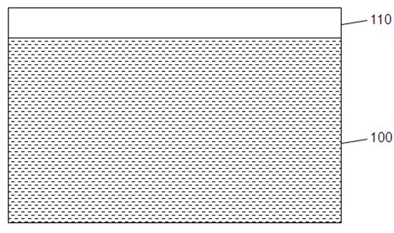
[0025] Such as figure 2 As shown, an N-type GaN-based semiconductor layer, an active layer and a P-type GaN-based semiconductor layer are epitaxially grown sequentially on a sapphire substrate 100 by metal organic chemical vapor deposition (MOCVD) to form a GaN-based epitaxial thin film 110 .

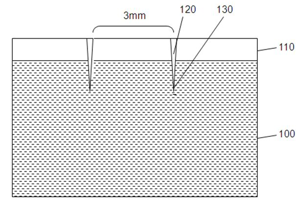
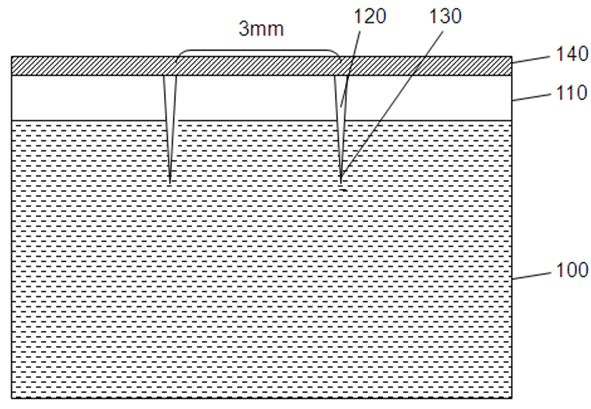
[0026] Such as image 3 As shown, the GaN-based epitaxial layer 110 is scribed and extended to the sapphire substrate 100 by using a laser scriber (wavelength 355nm). The size of the laser lift-off spot is similar, and the depth of the laser scribing is 30 microns, that is, to realize the GaN-based epitaxy unitization, the generated gas escape window 120, and the formation of the unit sapphire stress release point 130. The plan view is as foll


PUM


Abstract

The invention discloses a method for separating a sapphire substrate by unit on basis of stress action, comprising the following steps: adopting a first type of laser to realize the unit isolation of GaN base epitaxy; ensuring the unit independency of the GaN base epitaxy; meanwhile, utilizing a second type of laser to scan the upper tangential stress between the unit sapphire substrate and adjacent non-scanning unit sapphire substrate; and under the combined action of GaN interface nitrogen pressure and the upper tangential stress, separating and removing the sapphire substrate by unit. Thus, laser stripping finished product rate can be obviously improved.

Description


Claims


Application Information

Patent Timeline
Owner FUJIAN JING AN OPTOELECTRONICS CO LTD
Why Eureka
Try Eureka