Chip of light-emitting diode and preparation method thereof
A technology for light-emitting diodes and chips, applied in electrical components, circuits, semiconductor devices, etc., can solve the problems of small total reflection angle, inability to effectively improve the light extraction efficiency of chips, and low refractive index of semiconductor light-emitting materials. rate, avoid total reflection, improve the effect of luminous rate
- Summary
- Abstract
- Description
- Claims
- Application Information
AI Technical Summary
Problems solved by technology
Method used
Image

Examples
Embodiment 1
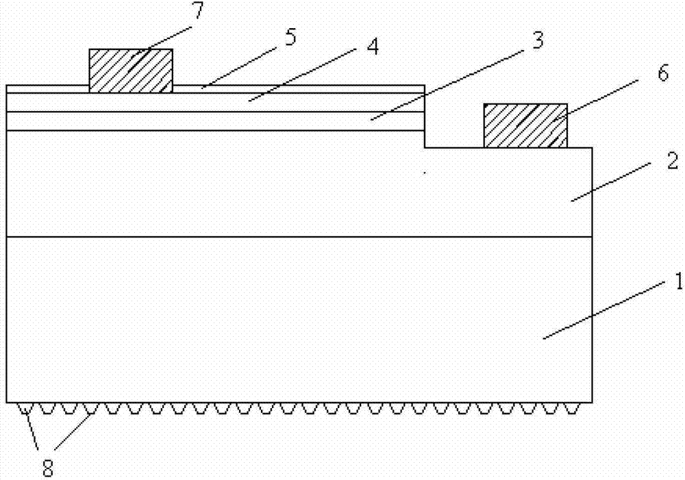
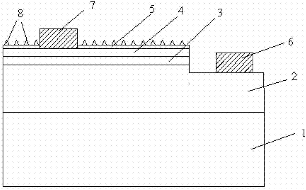
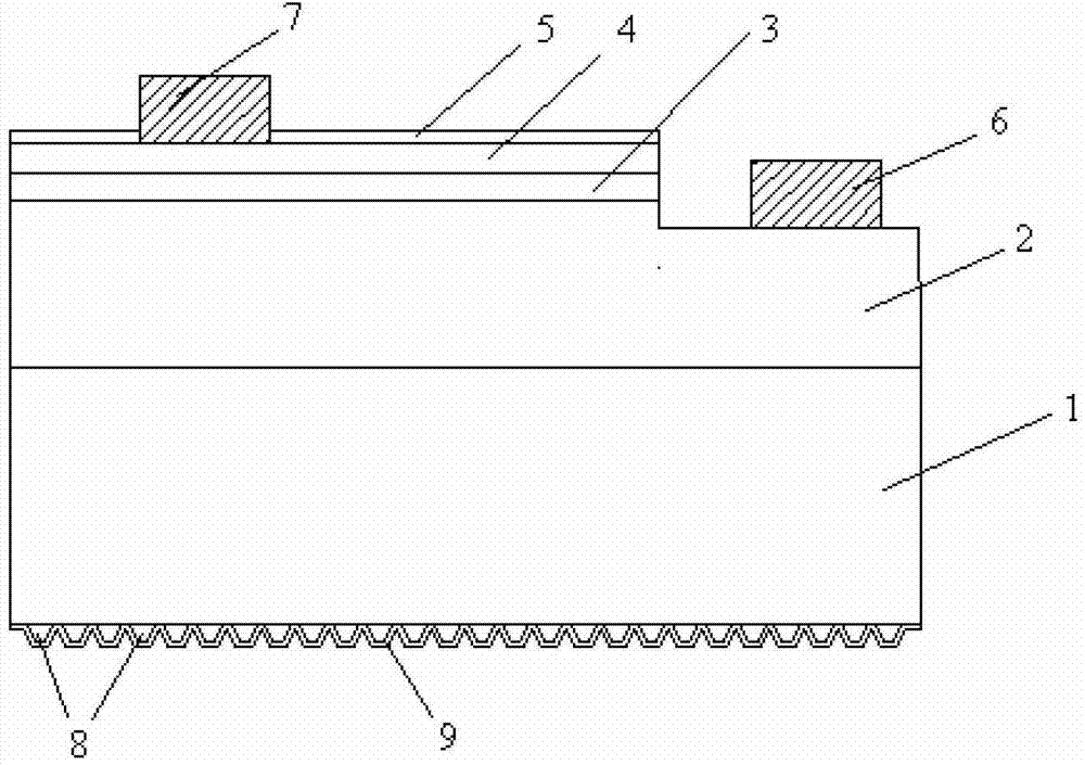
[0050] see figure 1 and figure 2, the embodiment of the present invention provides a LED chip, the chip includes: a substrate layer 1, an N-type layer 2 sequentially covered on the substrate layer 1, a light-emitting layer 3, a P-type layer 4 and a transparent conductive layer 5, and respectively The N electrode 6 and the P electrode 7 drawn out on the N type layer 2 and the P type layer 4 . Wherein, the chip further includes a transparent medium layer covering the bottom surface of the substrate layer 1 and / or the upper surface of the transparent conductive layer 5 . The refractive index of the transparent medium layer covering the bottom surface of the substrate layer 1 is higher than that of the substrate layer 1 ; the refractive index of the transparent medium layer covering the upper surface of the transparent conductive layer 5 is higher than that of the transparent conductive layer 5 .
[0051] Specifically, the substrate layer 1 includes a sapphire substrate, a silic
Embodiment 2
[0063] The embodiment of the present invention provides a method for preparing an LED chip, and the method flow includes:
[0064] 201: Provide a substrate layer, and sequentially grow an N-type layer, a light-emitting layer, a P-type layer, and a transparent conductive layer on the substrate layer.
[0065] 202: Prepare a wafer.
[0066] Among them, the preparation of the wafer includes: setting the N electrode and the P electrode on the N type layer and the P type layer respectively, and depositing a passivation layer on the transparent conductive layer, forming a transparent layer with a higher refractive index than the substrate layer on the bottom surface of the substrate layer. Dielectric layer made of transparent dielectric to obtain wafer. Or, form a transparent medium layer made of a transparent medium with a higher refractive index than the transparent conductive layer on the upper surface of the transparent conductive layer, set the N electrode and the P electrode on
Embodiment 3
[0071] The embodiment of the present invention provides a method for preparing an LED chip, and the method flow includes:
[0072] 301: Provide a substrate layer, and sequentially grow an N-type layer, a light-emitting layer, a P-type layer, and a transparent conductive layer on the substrate layer.
[0073] Specifically, an N-type layer 32, a light-emitting layer 33, a P-type layer 34, and a transparent conductive layer 35 can be grown on the substrate layer 31 by means of MOCVD (Metal-organic Chemical Vapor Deposition) (see Figure 4 ). This is a well-known technology in the art and will not be described in detail here.
[0074] Wherein, the substrate layer 31 may be a sapphire substrate, a silicon substrate, a silicon carbide substrate or a gallium nitride substrate.
[0075] In addition, the N-type layer 32, the light emitting layer 33, and the P-type layer 34 are all made of GaN.
[0076] 302: Arrange N electrodes and P electrodes on the N-type layer and P-type layer resp
PUM
| Property | Measurement | Unit |
|---|---|---|
| Height | aaaaa | aaaaa |
| Diameter | aaaaa | aaaaa |
| Thickness | aaaaa | aaaaa |
Abstract
Description
Claims
Application Information
 - R&D Engineer
- R&D Manager
- IP Professional
- Industry Leading Data Capabilities
- Powerful AI technology
- Patent DNA Extraction
Browse by: Latest US Patents, China's latest patents, Technical Efficacy Thesaurus, Application Domain, Technology Topic.
© 2024 PatSnap. All rights reserved.Legal|Privacy policy|Modern Slavery Act Transparency Statement|Sitemap