Method for manufacturing LED package

A technology for light-emitting diodes and manufacturing methods, which is applied to electrical components, electrical solid-state devices, circuits, etc., can solve the problems of long hardening time, large dispersion, low light decay, etc., and achieve the effects of low cost, few consumables, and low light decay.

Inactive Publication Date: 2013-08-21
江苏丰庆源科技有限公司
View PDF4 Cites 2 Cited by
  • Summary
  • Abstract
  • Description
  • Claims
  • Application Information

AI Technical Summary

Problems solved by technology

In order to make the LED chip produce white light, a small amount of phosphor powder is often mixed into the epoxy resin. The phosphor powder coated and filled in the liquid epoxy resin is not only dispersed in any direction, but also the liquid epoxy resin takes a long time to harden. Phosphors with a large specificity of epoxy resin will gather around the LED chip as time goes on, reduc

Method used


Image

  • Method for manufacturing LED package

Examples


Embodiment Construction

[0016] The method for manufacturing an LED light-emitting diode package according to the present invention will be further described in detail through specific embodiments below.

[0017] A method for manufacturing an LED light-emitting diode package, as follows:

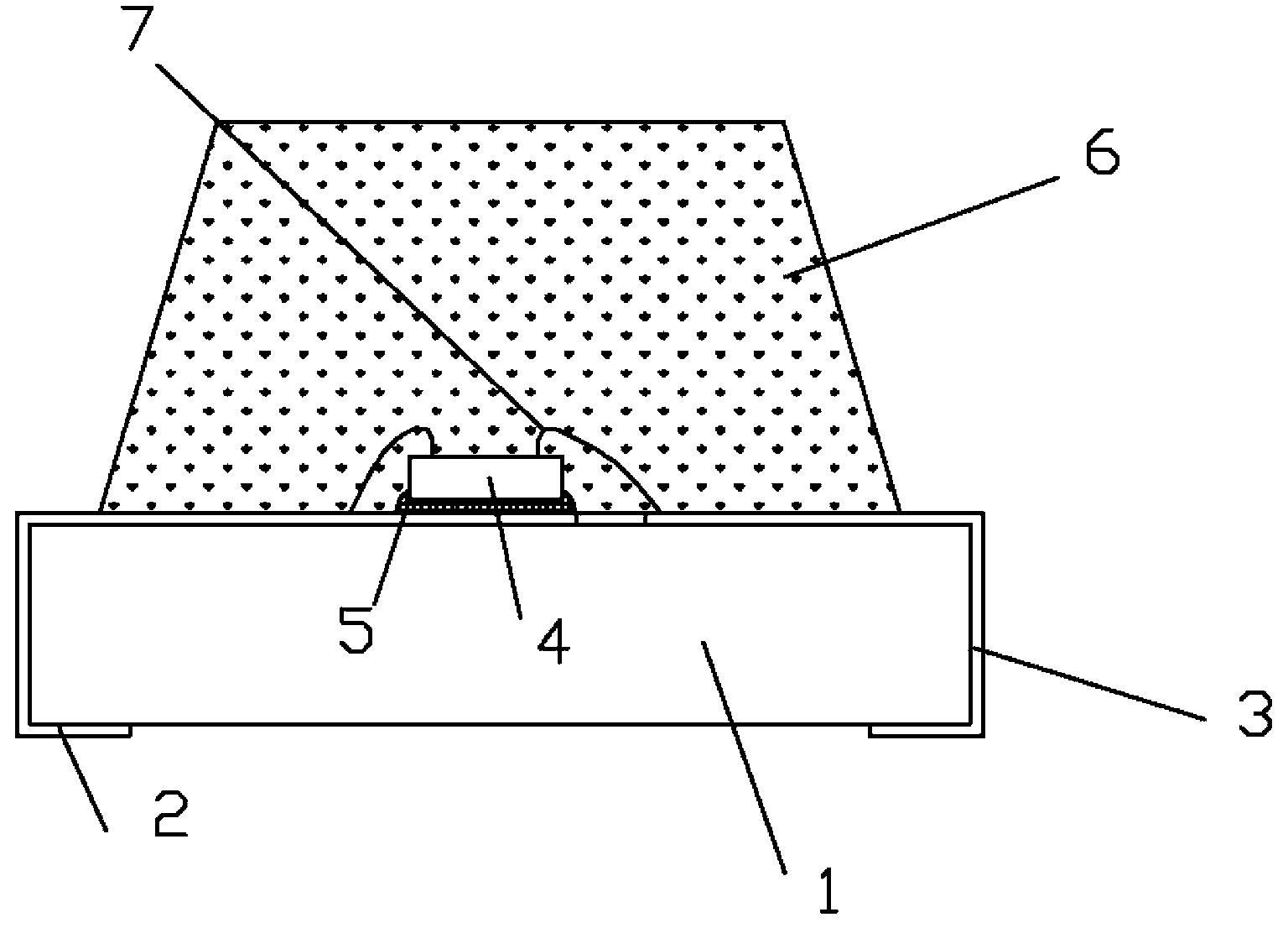
[0018] a. Install the positive electrode 2 and the negative electrode 3 on the printed circuit board 1 respectively;

[0019] b. bonding the LED chip 4 to the positive electrode 2 or the negative electrode 3 with glue, the positive pole and the negative pole of the LED chip 4 are electrically connected to the positive electrode 2 and the negative electrode 3 respectively, and the glue is hardened;

[0020] c. Place the transparent mold on the printed circuit board 1, make the LED chip 4 in the mold cavity of the transparent mold, fill the mold cavity with liquid silicone resin or a mixture of liquid silicone resin and phosphor powder, the filling is liquid silicone resin Or the mixture of liquid silicone resin and flu


PUM


Abstract

The invention discloses a method for manufacturing an LED package. The method includes the following steps: (1) positive electrodes and negative electrodes are respectively arranged on a printing circuit board; (2) LED chips are pasted on the positive electrodes or the negative electrodes through glue, positive poles and negative poles of the LED chips are electrically connected with the positive electrodes and the negative electrodes respectively, and the glue is hardened; (3) a transparent mould is placed on the printing circuit board, the LED chips are placed in an cavity of the transparent mould, mixtures of liquid silicon resin or liquid silicon resin and fluorescent powder are filled in the mould cavity, and the filling material is hardened to be a mould pressing forming portion; (4) the filling material is subjected to drying processing after being molded; (5) the transparent mould is moved out. The manufacturing method has the advantages that on one hand, less materials are used, cost is low, batch production can be achieved, and on the other hand, produced LED chips achieve the effects of high light effect, low light degradation and large light-emitting angle.

Description


Claims


Application Information

Patent Timeline
Owner 江苏丰庆源科技有限公司
Why Eureka
Try Eureka