Supporting and adsorbing jig for PCB

A technology for PCB boards and jigs, applied in the field of PCB board support adsorption jigs, can solve the problems of non-adjustable upper and lower positions of PCB boards, limited scope of application, and affecting the processing accuracy of PCB boards, and achieves wide application range, good versatility, The effect of improving accuracy

Inactive Publication Date: 2013-11-27
KUSN MAIZHI FIXTURE TECH
View PDF5 Cites 6 Cited by
  • Summary
  • Abstract
  • Description
  • Claims
  • Application Information

AI Technical Summary

Benefits of technology

This patented technology allows an electronic circuit (PC) card or other object to support its own weight while it moves along rails without being affected negatively. It also has two main technical features - one uses a special type called a padlock made of plastic material attached to each corner of the device's frame; another involves attaching a removable plate onto top of this padlock. By driving these parts together they allow movement between them, allowing precise adjustment over space needed for different processes like machining. Overall, this technology makes manufacturing more efficient and effective products possible.

Problems solved by technology

This patented describes an invention that allows for easy access to both top-down (height) positioning and bottom-up (length). However, current methods are often restricted by their ability to hold or fix certain parts of the circuit boards without changing them's overall dimensions. Additionally, these techniques have limitations with regard to how well they work when used over large areas such as power supply systems where temperature changes frequently occur due to fluctuations from outside temperatures.

Method used


Image

  • Supporting and adsorbing jig for PCB

Examples


Embodiment Construction

[0013] The present invention will be further described below in conjunction with the accompanying drawings.

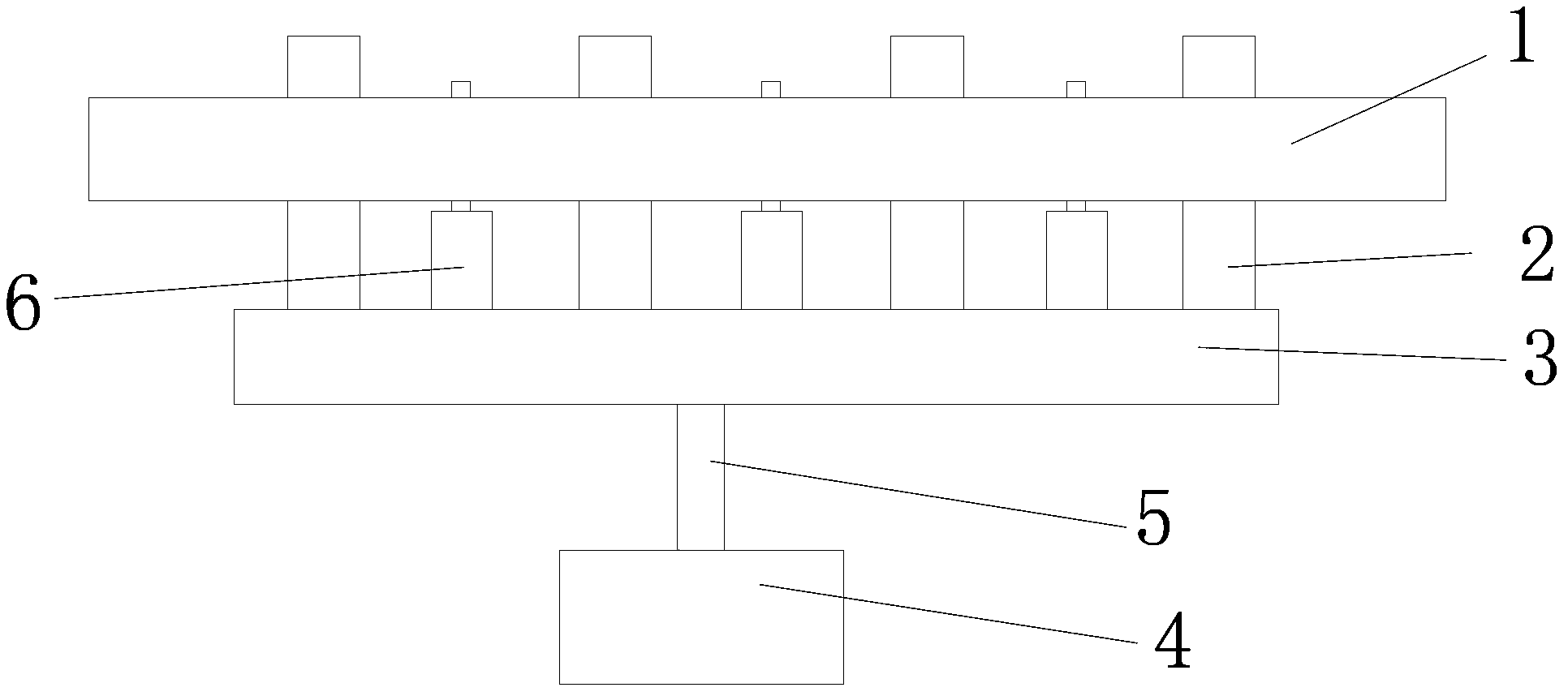
[0014] Such as figure 1 As shown, a PCB board support adsorption jig includes a rectangular base 1, a thimble 2, a moving plate 3, a cylinder 4, an adsorption nozzle 6 and a vacuum generator. The thimble 2 is connected with a moving plate 3 at the bottom of the thimble 2, the bottom of the moving plate 3 is connected with the cylinder rod 5 of the cylinder 4, and three adsorption nozzles 6 are arranged on the moving plate 3, and the corresponding position of the rectangular base 1 is provided with The through hole, the suction nozzle 6 can pass through the through hole, the length of the suction nozzle 6 is less than the length of the thimble 2, and the suction nozzle 6 is connected with the vacuum generator through a pipeline.

[0015] The thickness of the rectangular base 1 is 1 cm, the length of the thimble 2 is 3 cm, and the length of the suction nozzle 6 is 2.5 cm.


PUM

PropertyMeasurementUnit
Thicknessaaaaaaaaaa
Lengthaaaaaaaaaa

Abstract

The invention discloses a supporting and adsorbing jig for a PCB, which comprises a rectangular base, and is characterized in that a plurality of ejector pins capable of penetrating the rectangular base are arranged on the rectangular base; a movable board is connected to the bottoms of the ejector pins; the bottom of the movable board is connected with the cylinder rod of a cylinder; three adsorbing nozzles are arranged on the movable board; through holes are formed in the rectangular base in corresponding positions; the adsorbing nozzles can penetrate the through holes; the lengths of the adsorbing nozzles are shorter than those of the ejector pins; the adsorb nozzles are connected with a vacuum generator through pipelines. The conventional supporting and adsorbing jig for the PCB only can arrange the PCB in one height position, and the vertical position of the PCB cannot be adjusted, so that the application range is greatly limited; when the PCB is supported by the conventional supporting and adsorbing jig, the PCB can move during a machining process, so that the machining precision of the PCB is greatly impacted. The supporting and adsorbing jig provided by the invention has the advantages that the problems of the conventional supporting and adsorbing jig are solved; the structure is simple; the supporting height can be adjusted; the right position of the PCB can be kept.

Description


Claims


Application Information

Patent Timeline
Owner KUSN MAIZHI FIXTURE TECH
Why Eureka
Try Eureka