Preparation method of 3D peripheral grid MOS tube
A technology of MOS tube and surrounding gate, which is used in semiconductor/solid-state device manufacturing, electrical components, circuits, etc., can solve the problems of complex epitaxy process, achieve high performance, improve integration and easy operation.
- Summary
- Abstract
- Description
- Claims
- Application Information
AI Technical Summary
Benefits of technology
Problems solved by technology
Method used
Image

Examples
Embodiment Construction
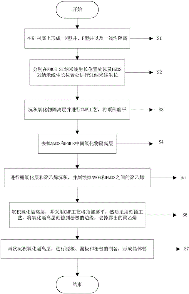
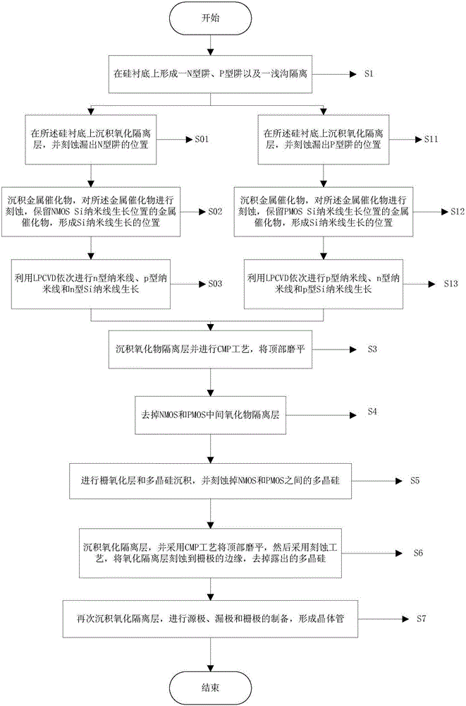
[0046] A method for manufacturing a 3D peripheral gate MOS transistor according to the present invention will be described in detail below in conjunction with the accompanying drawings and specific embodiments.
[0047] Such as Figure 1 ~ 3O As shown, a method for preparing a 3D surrounding gate MOS transistor comprises steps:
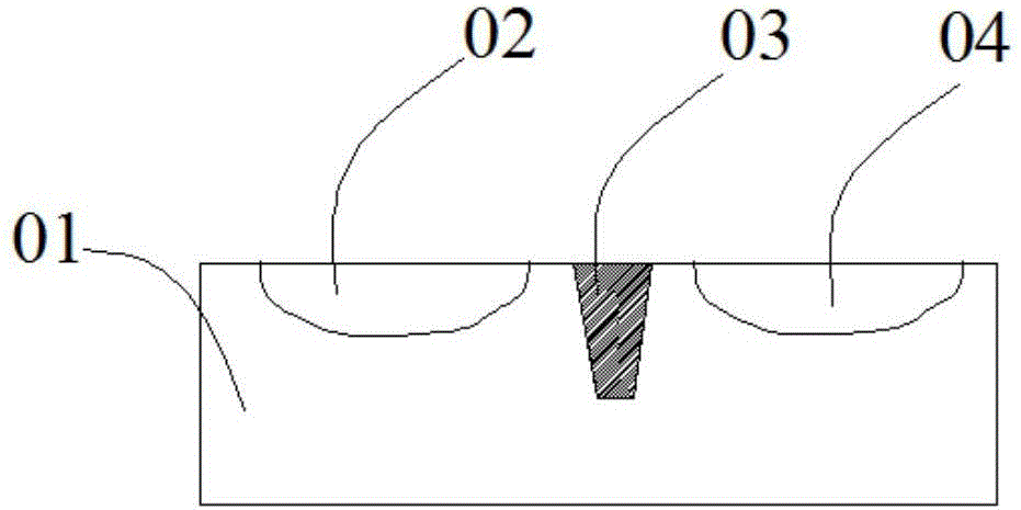
[0048] S1: Form an N-type well 02, a P-type well 04, and a shallow trench isolation 03 on the silicon substrate 01, and the shallow trench isolation 03 is located between the N-type well 02 and the P-type well 04, so that the N-type Well 02 is isolated from P-type well 04;
[0049] S2: growing silicon nanowires at the growth position of the NMOS silicon nanowires (ie above the N-type well 02) and at the growth position of the PMOS silicon nanowires (ie above the P-type well 04);
[0050] S3: Depositing an oxide isolation layer 1 and performing a CMP process, and smoothing the oxide isolation layer on the top of the silicon nanowire;
[0051] S4: remov
PUM
| Property | Measurement | Unit |
|---|---|---|
| Thickness | aaaaa | aaaaa |
| Thickness | aaaaa | aaaaa |
| Thickness | aaaaa | aaaaa |
Abstract
Description
Claims
Application Information
 - R&D Engineer
- R&D Manager
- IP Professional
- Industry Leading Data Capabilities
- Powerful AI technology
- Patent DNA Extraction
Browse by: Latest US Patents, China's latest patents, Technical Efficacy Thesaurus, Application Domain, Technology Topic.
© 2024 PatSnap. All rights reserved.Legal|Privacy policy|Modern Slavery Act Transparency Statement|Sitemap