Pixel structure, method for driving pixel structure, display substrate and display panel

A pixel structure and pixel electrode technology, applied in nonlinear optics, instruments, optics, etc., can solve the problems of reducing the charging and discharging efficiency of the pixel electrode, increasing the charging time of the pixel electrode, etc., so as to improve the charging and discharging efficiency and shorten the charging time. effect of time

Inactive Publication Date: 2016-09-28
BOE TECH GRP CO LTD +1
View PDF8 Cites 3 Cited by
  • Summary
  • Abstract
  • Description
  • Claims
  • Application Information

AI Technical Summary

Benefits of technology

This technology allows for faster charging times with direct addressable pixels without having to scan their entire screen or slow down its operation.

Problems solved by technology

This patented technology describes how in order to improve image quality by improving charging speed during displaying images with Thinfilm Liquid Crystals Display devices (TFT LC Displays). However, this process requires that certain parts or elements within pixels have been completely charged before they start being driven again once new frames appear. Additionally, there needs some way to quickly remove these partially charged areas from the device's screen without affecting its performance negatively.

Method used


Image

  • Pixel structure, method for driving pixel structure, display substrate and display panel
  • Pixel structure, method for driving pixel structure, display substrate and display panel
  • Pixel structure, method for driving pixel structure, display substrate and display panel

Examples


Embodiment Construction

[0026] In order for those skilled in the art to better understand the technical solution of the present invention, the pixel structure and its driving method, display substrate and display panel provided by the present invention will be described in detail below with reference to the accompanying drawings.

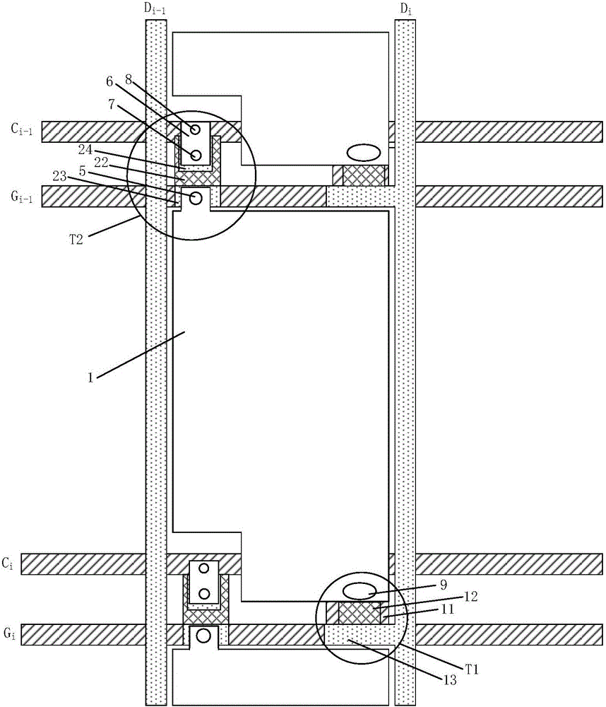
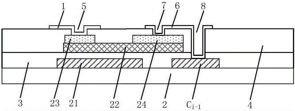
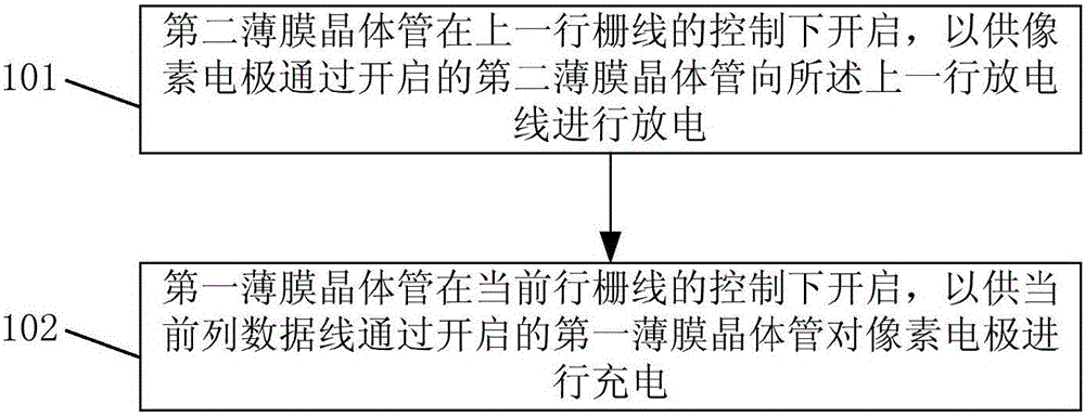
[0027] figure 1 A schematic structural diagram of a pixel structure provided in Embodiment 1 of the present invention, as shown in figure 1 As shown, the pixel structure includes: a first thin film transistor T1, a second thin film transistor T2 and a pixel electrode 1, and the first thin film transistor T1 is connected to the current row gate line G i , the current column data line D i and the pixel electrode 1, the second thin film transistor T2 is connected to the gate line G of the last row i-1 , the last line of discharge line C i-1 and pixel electrode 1. The second thin film transistor T2 is used in the upper row of gate line G i-1 It is turned on under the control


PUM


Abstract

The invention discloses a pixel structure, a method for driving the pixel structure, a display substrate and a display panel. The pixel structure comprises a first thin film transistor, a second thin film transistor and a pixel electrode, wherein the first thin film transistor is connected to a grid line on the current line, a data line on the current row, and a pixel electrode, and the second thin film transistor is connected to a grid line on the previous line, a discharge line on the previous line, and the pixel electrode; the second thin film transistor is used for being switched on under the control of the grid line on the previous line, so that the pixel electrode can conduct discharging on the discharge line on the previous line through the second thin film transistor which is switched on; the first thin film transistor is used for being switched on under the control of the grid line on the current line, so that the data line on the current row can conduct charging on the pixel electrode through the first thin film transistor which is switched on. The charging and discharging efficiency of the pixel electrode is improved.

Description


Claims


Application Information

Patent Timeline
Owner BOE TECH GRP CO LTD
Why Eureka
Try Eureka