Radio frequency switching circuit with improved bias circuit

A radio frequency switch and bias voltage technology, applied in the field of radio frequency circuits, can solve the problems of increased chip cost and large area, and achieve the effect of saving chip area and reducing cost

Inactive Publication Date: 2017-04-26
WUXI ZHONGPU MICROELECTRONICS CO LTD
View PDF8 Cites 0 Cited by
  • Summary
  • Abstract
  • Description
  • Claims
  • Application Information

AI Technical Summary

Benefits of technology

The current method for controlling an electronic device's power supply involves utilizing two different voltages: one higher (positive) compared to ground levels; another lower called "negative". This allows more space on the die without requiring extra components like capacitors that are expensive at larger sizes.

Problems solved by technology

This patented problem addressed in this patents relates to improving the performance of electronic devices such as radios or communication systems due to their use of semiconductor technology called Silicone On Insulators Technology (SOT). These technologies allow signals transmitted through waveguides without being affected by external electromagnetic interference from other sources like microwaves or wireless networks. To improve these technical effects, there has been proposed various solutions involving generating negative pressures during operation while avoiding any unwanted side effect on sensitive components within the device's structure.

Method used


Image

  • Radio frequency switching circuit with improved bias circuit
  • Radio frequency switching circuit with improved bias circuit
  • Radio frequency switching circuit with improved bias circuit

Examples


Embodiment Construction

[0029] In order to make the above objects, features and advantages of the present invention more comprehensible, the present invention will be further described in detail below in conjunction with the accompanying drawings and specific embodiments.

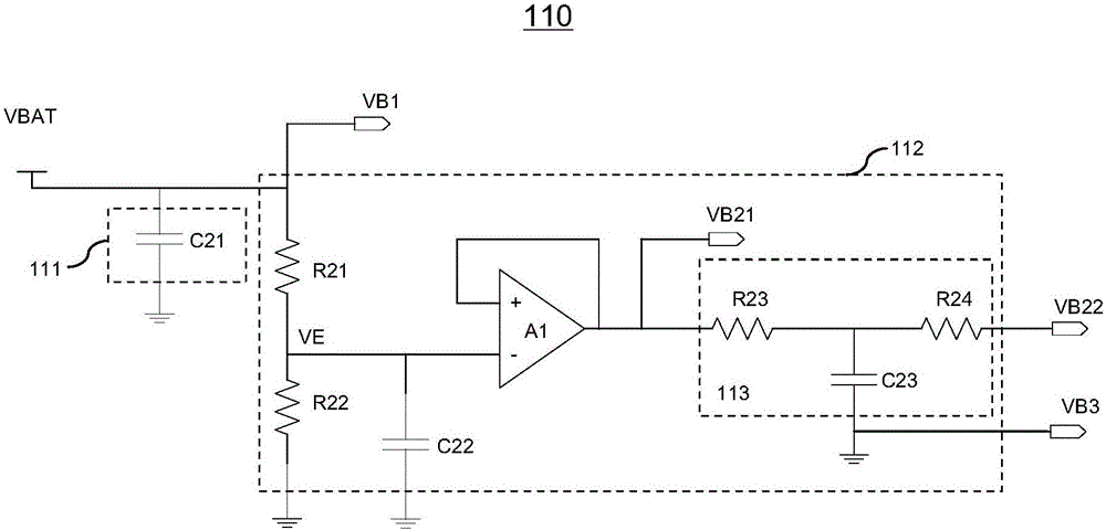
[0030] The invention provides a radio frequency switch circuit with an improved bias circuit. The bias of the radio frequency switch can be realized without setting a negative pressure charge pump in the bias circuit, thereby saving chip area and reducing cost.

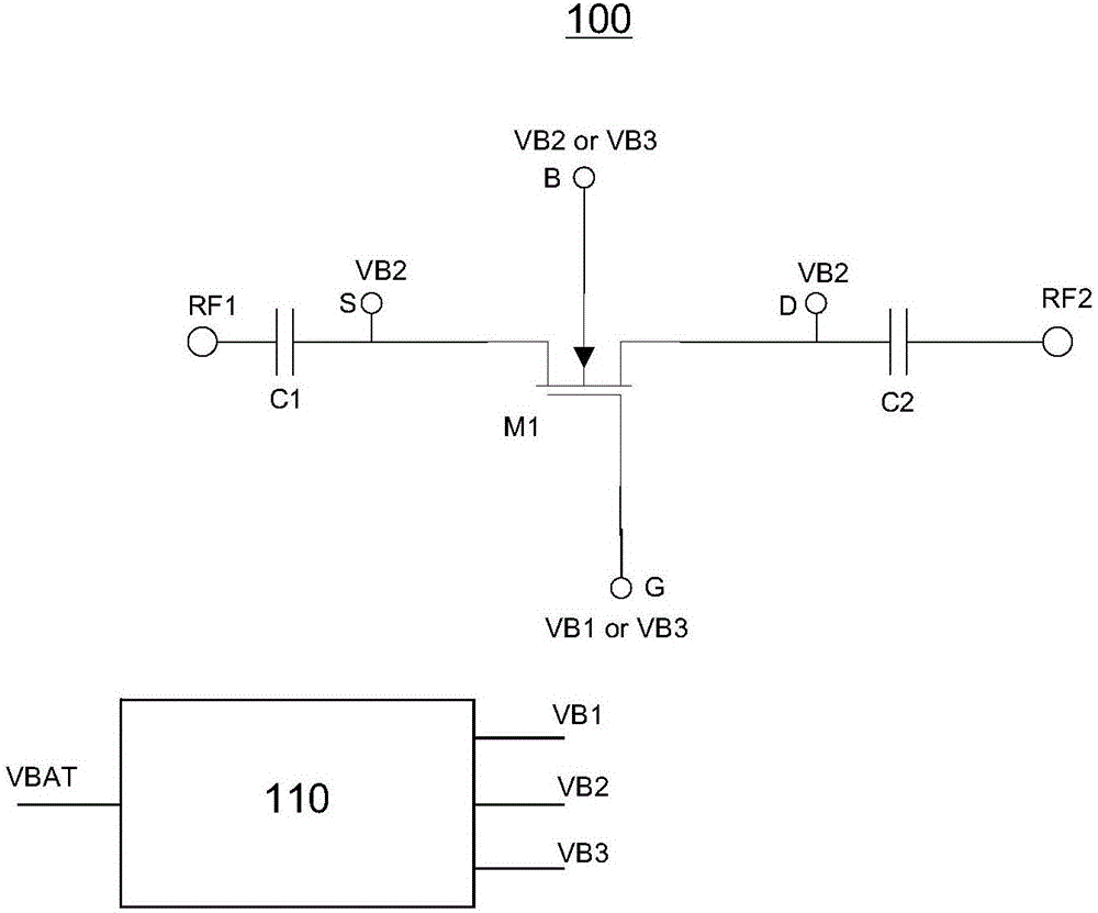
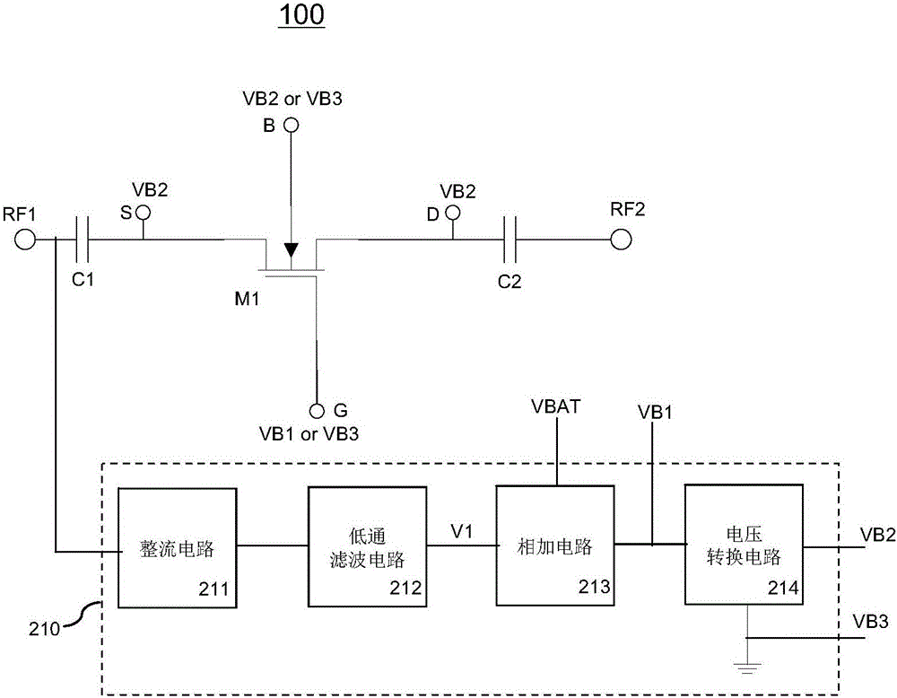
[0031] figure 1 A circuit diagram of an embodiment of the radio frequency switch circuit 100 in the present invention is shown. Such as figure 1 As shown, the radio frequency switch circuit 110 includes a first radio frequency terminal RF1 , a second radio frequency terminal RF2 , a first capacitor C1 , a second capacitor C2 , a radio frequency switch M1 and a bias circuit 110 . When the radio frequency switch M1 is turned on, the radio frequency signal can be transmitted


PUM


Abstract

The present invention discloses a radio frequency switching circuit with an improved bias circuit. The radio frequency switching circuit comprises a first radio frequency end, a second radio frequency end, a first capacitor, a second capacitor, a radio frequency switch and a bias circuit; the radio frequency switch includes a source, a drain, a gate and an end body, wherein the source is coupled to the first radio frequency end through the first capacitor, the drain is coupled to the second radio frequency end through the second capacitor; and the bias circuit provides first bias voltage, second bias voltage and third bias voltage based on battery voltage, wherein the first bias voltage is larger than the second bias voltage, the second bias voltage is larger than the third bias voltage, and the second bias voltage is coupled to the source and drain of the radio frequency switch; when the radio frequency switch is required to be controlled to be switched on, the first bias voltage is coupled to the gate of the radio frequency switch, and the second bias voltage is coupled to the end body end of the radio frequency switch; and when the radio frequency switch is required to be controlled to be switched off, the third bias voltage is coupled to the gate and end body of the radio frequency switch. Thus, the area of a chip can be decreased, and costs can be reduced.

Description


Claims


Application Information

Patent Timeline
Owner WUXI ZHONGPU MICROELECTRONICS CO LTD
Why Eureka
Try Eureka