Device and method for detecting surface imperfection of curved-surface optical element

An optical element and detection device technology, applied in the field of optical detection, can solve the problems of reduced accuracy, open air bubbles, visual fatigue, etc., and achieve the effects of low cost and simple structure

Pending Publication Date: 2018-06-12
HEFEI ZHICHANG PHOTOELECTRIC TECH
View PDF15 Cites 4 Cited by
  • Summary
  • Abstract
  • Description
  • Claims
  • Application Information

AI Technical Summary

Benefits of technology

This technology uses an LED lamp or laser diode (LD) for providing uniform brightness over large areas like windows. It also includes a special lens made up of multiple layers of glass placed between two sheets of clear plastic called polyethylene terephthate (PET). By shining this mirror onto these surfaces at certain angles, it becomes possible to see how bent things look inside them without being noisy due to their bending nature. Additionally, there're some ways to measure its shape accurately through cameras attached to mobile devices such as smart phones.

Problems solved by technology

This patents describes an issue with detecting surface flaws during manufacturing processes when producing high-quality flat surfaces like glass or plastic panels that require precise alignment between parts. Manual inspectors can be time-consuming and subjective due to their ability to distinguish small differences from large variations caused by external factors like temperature changes over time. There have been attempts at developing automated methods for accurately identifying cracks and other issues associated with curved materials. However, current automatic techniques cannot effectively identify even minute imperfections which may lead to reduced functionality and reliability of the final product.

Method used


Image

  • Device and method for detecting surface imperfection of curved-surface optical element
  • Device and method for detecting surface imperfection of curved-surface optical element
  • Device and method for detecting surface imperfection of curved-surface optical element

Examples


Embodiment 1

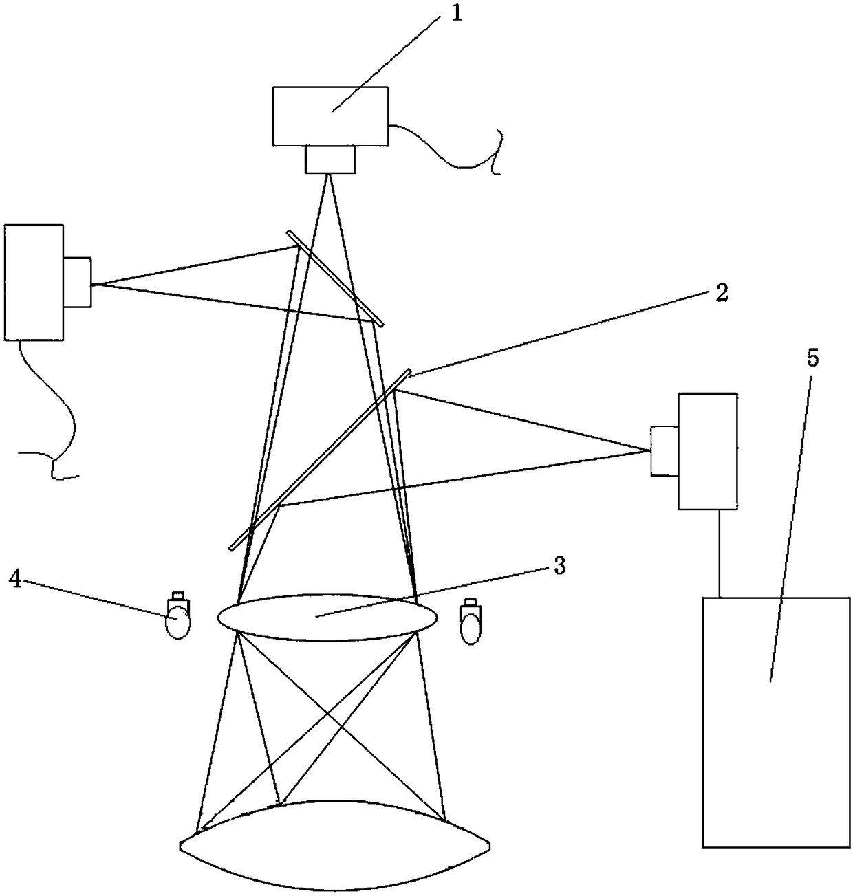
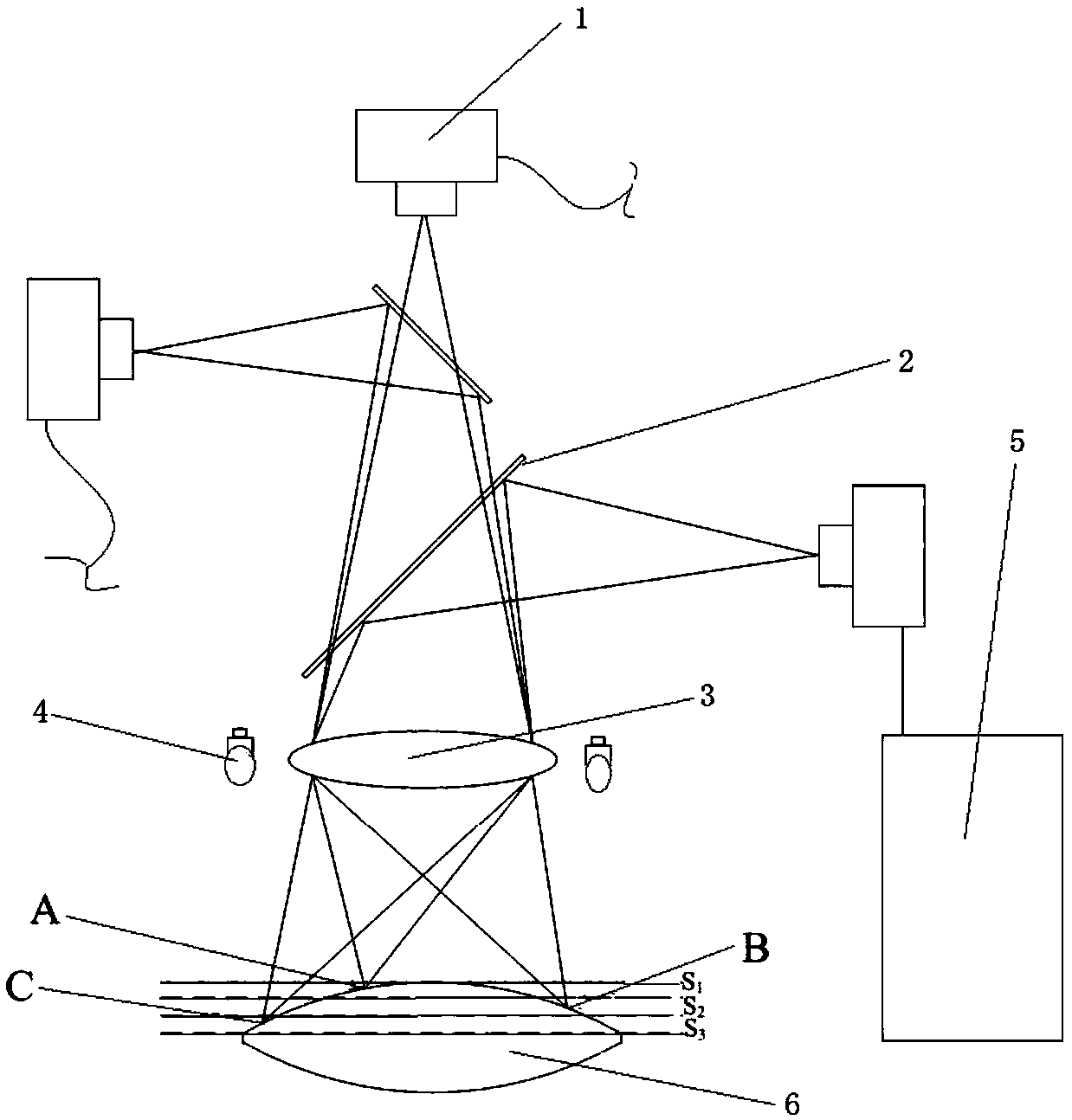
[0024] see Figure 1-2 , in an embodiment of the present invention, a device for detecting surface defects of a curved optical element includes an illumination system and an imaging system. The imaging system is provided with an imaging lens 3, an imaging device, and a processor 3 connected to the imaging device for signals. The device has three groups, including one group of coaxial imaging mechanism and two groups of side imaging mechanism, the axial imaging mechanism includes a third camera sensor located above the imaging lens 3 and coaxial with the imaging lens 3, the side imaging mechanism includes a The first camera sensor on the right side of the imaging lens 3 and the second camera sensor arranged on the left side of the imaging lens 3, the axis of the first camera sensor and the axis of the imaging lens 3 are vertically intersected and at the point of intersection, an angle of 45° with the horizontal is provided. The first visible light part reflector, and the reflectiv

Embodiment 2

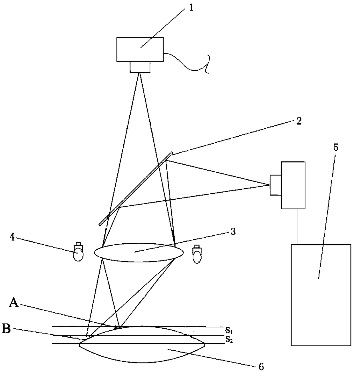
[0027] see image 3 , compared with Embodiment 1, the present embodiment measures the difference of the curved surface optical element at all, and a group of axial imaging mechanism and a group of side imaging mechanism are set, and the reflectivity of the visible light partial reflector 2 in the side imaging mechanism is 50%. , the rest of the structure and detection process are the same as in Embodiment 1.


PUM


Abstract

The invention discloses a device for detecting the surface imperfection of a curved-surface optical element. The device comprises a lighting system and an imaging system and is characterized in that light sources are arranged in the lighting system, the imaging system comprises an imaging lens, an imaging device and a processor in signal connection with the imaging device, the light sources are arranged outside the imaging lens, and the imaging device at least comprises a coaxial imaging mechanism or a lateral imaging mechanism. The device has the advantages that on the basis of the light scattering principle, the light source evenly irradiates the surface of the curved-surface optical element, the imaging system above the curved-surface optical element detects the imaging of the curved-surface optical element, the curved-surface optical elements of different curvature radiuses can be detected, the difficulty that the surface imperfection of the curved-surface optical element cannot beautomatically detected is solved, and the device is low in cost and simple in structure.

Description


Claims


Application Information

Patent Timeline
Owner HEFEI ZHICHANG PHOTOELECTRIC TECH
Why Eureka
Try Eureka