Surface acoustic wave device impedance matcher
An impedance matcher and surface acoustic wave technology, applied in impedance networks, electrical components, etc., can solve problems such as limiting the effectiveness of filters, and the inability of filters to effectively use high-frequency wireless communication equipment to reduce insertion loss and noise. coefficient, the effect of reducing the occupied area
- Summary
- Abstract
- Description
- Claims
- Application Information
AI Technical Summary
Problems solved by technology
Method used
Image

Examples
Embodiment 1
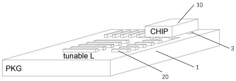
[0046] Such as figure 1 As shown, the present embodiment provides a surface acoustic wave device impedance matching device, comprising: a circuit substrate (1), having opposite upper and lower surfaces; a surface acoustic wave device (10), and the circuit substrate (1) A gap is formed between the upper surfaces of the upper surfaces; bumps (3), the surface acoustic wave device (10) is arranged on the upper surface of the circuit substrate (1) through the bumps (3); the surface acoustic wave device of the present invention The device can be SAW, XBAR, etc., and the surface acoustic wave device is packaged in a flip-chip packaging manner, and the side with the IDT electrode is arranged in the gap formed between the surface acoustic wave device and the first surface of the circuit substrate, thereby avoiding the sealing material For example, the resin or the substrate surface is in contact with the IDT electrodes, so as to avoid affecting the sensitive IDT electrodes. In order to p
Embodiment 2
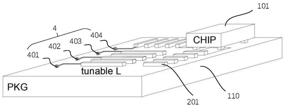
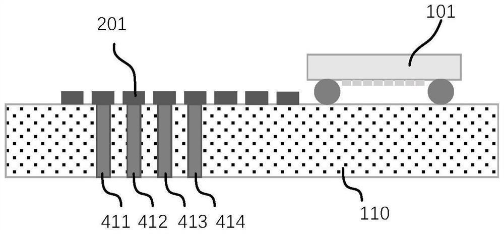
[0050] Such as figure 2 As shown, this embodiment is further improved on the basis of Embodiment 1, specifically comprising: a circuit substrate (110) having opposite upper and lower surfaces; a surface acoustic wave device (101), and the circuit substrate A gap is formed between the upper surfaces of (110); bumps, the surface acoustic wave device (101) is arranged on the upper surface of the circuit substrate (110) through the bumps; a plurality of metal electrodes (201), set The upper surface of the circuit substrate (110) is electrically coupled with the bump through wires for impedance matching with an external circuit. An impedance matching terminal (4) is also provided, figure 2 Four impedance matching terminals (401, 402, 403, 404) are exemplarily shown in , but the present invention is not limited thereto. The impedance matching terminal (4) is arranged on the upper surface of the circuit substrate (110), and is electrically coupled with the metal electrode (201), so
Embodiment 3
[0055] Such as Figure 7 As shown, this embodiment provides an impedance matcher for a surface acoustic wave device. The impedance matcher for a surface acoustic wave device in this embodiment is similar to the impedance matcher for a surface acoustic wave device in Embodiment 2. The upper surface of the circuit substrate (111) A metal electrode (30) is provided, the difference is that on the basis of the second embodiment, an input terminal, an output terminal and a grounding structure are also provided on the upper surface of the circuit substrate (111), and the metal electrode (30) Electrically coupled to the input terminal, output terminal and ground structure to provide input signals to and output signals from the surface acoustic wave device (110). The input terminal, the output terminal, the grounding structure and the impedance matching terminal of the metal electrode (30) all extend to the lower surface of the circuit substrate (111) through the via hole to form the inpu
PUM
| Property | Measurement | Unit |
|---|---|---|
| Thermal conductivity at room temperature | aaaaa | aaaaa |
Abstract
Description
Claims
Application Information
 - R&D Engineer
- R&D Manager
- IP Professional
- Industry Leading Data Capabilities
- Powerful AI technology
- Patent DNA Extraction
Browse by: Latest US Patents, China's latest patents, Technical Efficacy Thesaurus, Application Domain, Technology Topic.
© 2024 PatSnap. All rights reserved.Legal|Privacy policy|Modern Slavery Act Transparency Statement|Sitemap