Test point identification method and device and application
An identification method and test point technology, applied in special data processing applications, instruments, geometric CAD, etc., can solve problems such as consuming the energy of technicians, affecting production efficiency, and missed inspections, reducing testing and improving testing efficiency.
- Summary
- Abstract
- Description
- Claims
- Application Information
AI Technical Summary
Benefits of technology
Problems solved by technology
Method used
Image

Examples
Embodiment 1
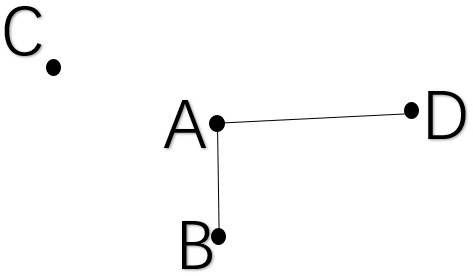
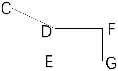
[0033] The embodiments of the present application provide a method for identifying test points, which can accurately identify necessary test points on a printed circuit board, reduce testing of unnecessary test points, and improve the test efficiency of printed circuit boards. Specifically, refer to figure 1 , the method includes:
[0034] Obtaining a PCB basic primitive, wherein the PCB basic primitive includes a network node and a network line segment connecting the network node;
[0035] A network connectivity graph is constructed based on the PCB basic primitives, wherein any two of the PCB basic primitives in each of the network connectivity graphs are connected;
[0036] Select any network node in the network connectivity graph as the execution node, take the execution node as the starting point to travel the network connectivity graph, mark the traveled network node as the traveled node during the travel process, and mark the traveled network segment as the traveled node.
Embodiment 2
[0068] Based on the same idea, refer to Figure 7 , the application also proposes a test point identification device, including:
[0069] A primitive acquiring unit 301 is configured to acquire a PCB basic primitive, wherein the PCB basic primitive includes a network node and a network line segment connecting the network node;
[0070] A network connectivity graph obtaining unit 302, configured to construct a network connectivity graph based on the PCB basic primitives, wherein any two of the PCB basic primitives in each of the network connectivity graphs are connected;
[0071] The tour unit 303 is configured to select any network node in the network connectivity graph as an execution node, and travel the network connectivity graph with the execution node as a starting point, and mark the traveled network node as a traveled node during the travel process, and mark the traveled network node as a traveled node. The traveled network line segment is a traveled line segment, and the
Embodiment 3
[0075] This embodiment also provides an electronic device, refer to Figure 8 , which includes a memory 404 and a processor 402, where a computer program is stored in the memory 404, and the processor 402 is configured to run the computer program to execute the steps in any of the above-mentioned embodiments of the test point identification method.
[0076] Specifically, the above-mentioned processor 402 may include a central processing unit (CPU), or a specific integrated circuit (Application Specific Integrated Circuit, ASIC for short), or may be configured as one or more integrated circuits implementing the embodiments of the present application.
[0077]Among others, memory 404 may include mass storage 404 for data or instructions. By way of example and not limitation, the memory 404 may include a hard disk drive (Hard Disk Drive, abbreviated as HDD), a floppy disk drive, a solid state drive (Solid State Drive, abbreviated as SSD), flash memory, optical disk, magneto-optical
PUM
 Abstract
Description
Claims
Application Information
 - R&D Engineer
- R&D Manager
- IP Professional
- Industry Leading Data Capabilities
- Powerful AI technology
- Patent DNA Extraction
Browse by: Latest US Patents, China's latest patents, Technical Efficacy Thesaurus, Application Domain, Technology Topic.
© 2024 PatSnap. All rights reserved.Legal|Privacy policy|Modern Slavery Act Transparency Statement|Sitemap