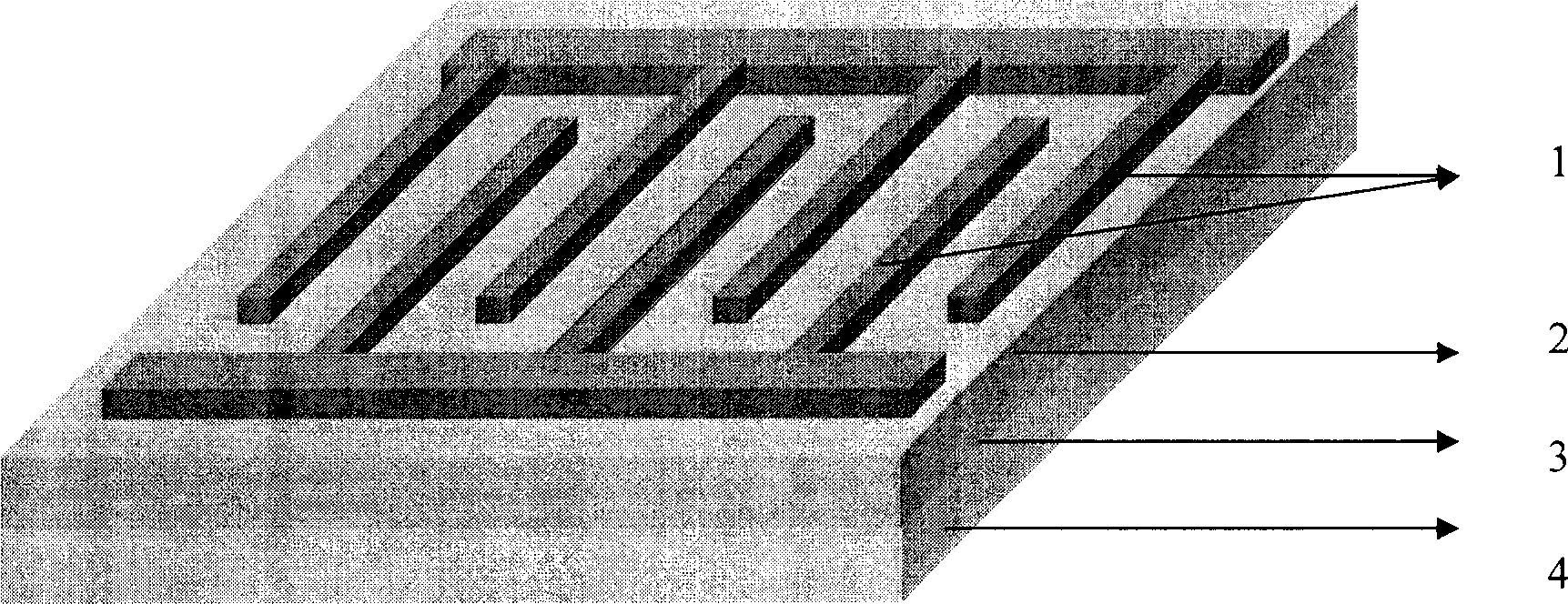
Metal/semiconductor/metallic structure TiO2 ultraviolet photodetector and preparation
A metal structure, detector technology, applied in semiconductor devices, final product manufacturing, sustainable manufacturing/processing, etc., can solve problems such as complex reaction processes
- Summary
- Abstract
- Description
- Claims
- Application Information
AI Technical Summary
Problems solved by technology
Method used
Image

Examples
Embodiment 1
[0053] A:
[0054] a. Put 10mL of Ti(OC 4 h 9 ) 4 Add it dropwise to 100mL of absolute ethanol under vigorous stirring, then add dropwise 10mL of glacial acetic acid, and after 30min of stirring, a uniform and transparent light yellow solution is obtained; slowly add 10mL of deionized water to the above-mentioned solution at a rate of 2mL / min In the solution, continue to stir for 1 h to obtain a uniform and transparent light yellow sol, and place it for aging for 3 h for later use;
[0055] b. Use aged sol to grow SiO 2 Preparation of TiO on Si substrate 2 Thin film, the film thickness is 0.2μm, the film is made by spin coating method, and the rotation speed is 2500rpm;
[0056] c. Finally, put the film into a muffle furnace for calcination, the temperature is controlled at 650°C, and the calcination time is 2 hours. After that, the power is turned off and the film is naturally cooled to room temperature with the furnace.
[0057] B:
[0058] In nanocrystalline TiO 2 Th
Embodiment 2
[0075] A:
[0076] a. Put 10mL of Ti(OC 4 h 9 ) 4 Add it dropwise to 100mL of absolute ethanol under vigorous stirring, then add dropwise 10mL of glacial acetic acid, and after 30min of stirring, a uniform and transparent light yellow solution is obtained; slowly add 10mL of deionized water to the above-mentioned solution at a rate of 2mL / min In the solution, continue to stir for 1 h to obtain a uniform and transparent light yellow sol, and place it for aging for 3 h for later use;
[0077] b. Use aged sol to grow SiO 2 Preparation of TiO on Si substrate 2 Thin film, the film thickness is 0.18μm, the film is made by spin coating method, and the rotation speed is 3000rpm;
[0078] c. Finally, put the film into a muffle furnace for calcination, the temperature is controlled at 600°C, and the calcination time is 2 hours. After that, the power is turned off and the film is naturally cooled to room temperature with the furnace.
[0079] B:
[0080] In nanocrystalline TiO 2 T
Embodiment 3
[0097] A:
[0098] a. Put 10mL of Ti(OC 4 h 9 ) 4 Add dropwise into 100mL of absolute ethanol under vigorous stirring, then dropwise add 10mL of glacial acetic acid, after 30min of stirring, a uniform and transparent light yellow solution is obtained; slowly add 10mL of deionized water to the above-mentioned solution at a rate of 2mL / min In the solution, continue to stir for 1 h to obtain a uniform and transparent light yellow sol, and place it for aging for 3 h for later use;
[0099] b. Use aged sol to grow SiO 2 Preparation of TiO on Si substrate 2 Thin film, the thickness of the film is 180nm, the method of spin coating is used for film formation, and the rotation speed is 3000rpm;
[0100] c. Finally, put the film into a muffle furnace for calcination, the temperature is controlled at 600°C, and the calcination time is 2 hours. After that, the power is turned off and the film is naturally cooled to room temperature with the furnace.
[0101] B:
[0102] Using tin foil
PUM
| Property | Measurement | Unit |
|---|---|---|
| Thickness | aaaaa | aaaaa |
| Thickness | aaaaa | aaaaa |
| Width | aaaaa | aaaaa |
Abstract
Description
Claims
Application Information
 - R&D Engineer
- R&D Manager
- IP Professional
- Industry Leading Data Capabilities
- Powerful AI technology
- Patent DNA Extraction
Browse by: Latest US Patents, China's latest patents, Technical Efficacy Thesaurus, Application Domain, Technology Topic.
© 2024 PatSnap. All rights reserved.Legal|Privacy policy|Modern Slavery Act Transparency Statement|Sitemap