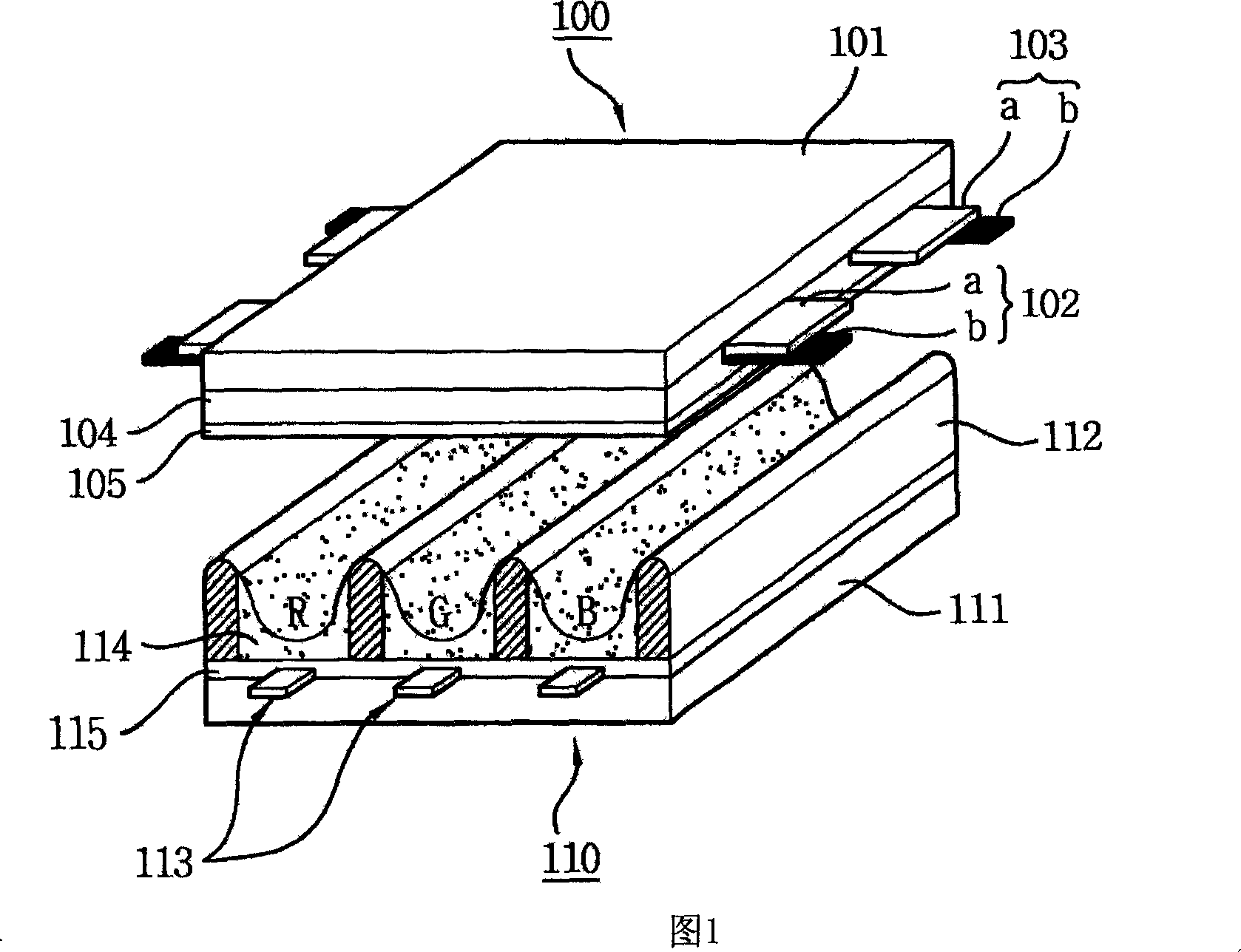
Positioning sign forming method for plasma display panel
A positioning mark and display panel technology, applied to instruments, identification devices, etc., can solve the problems of time-consuming, complicated AlignMark etching operation, and difficult modification of AlignMark, so as to reduce the formation time and error, reduce the number of movements, and simplify the etching operation Effect
- Summary
- Abstract
- Description
- Claims
- Application Information
AI Technical Summary
Problems solved by technology
Method used
Image

Examples
Example Embodiment
[0036] Hereinafter, the present invention will be described in detail with reference to the drawings.
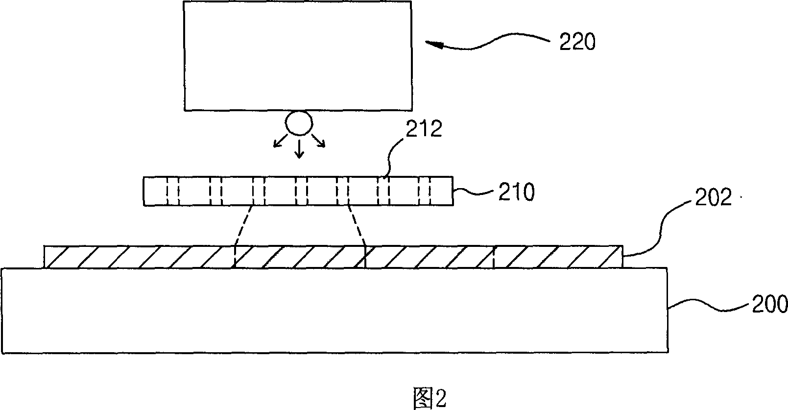
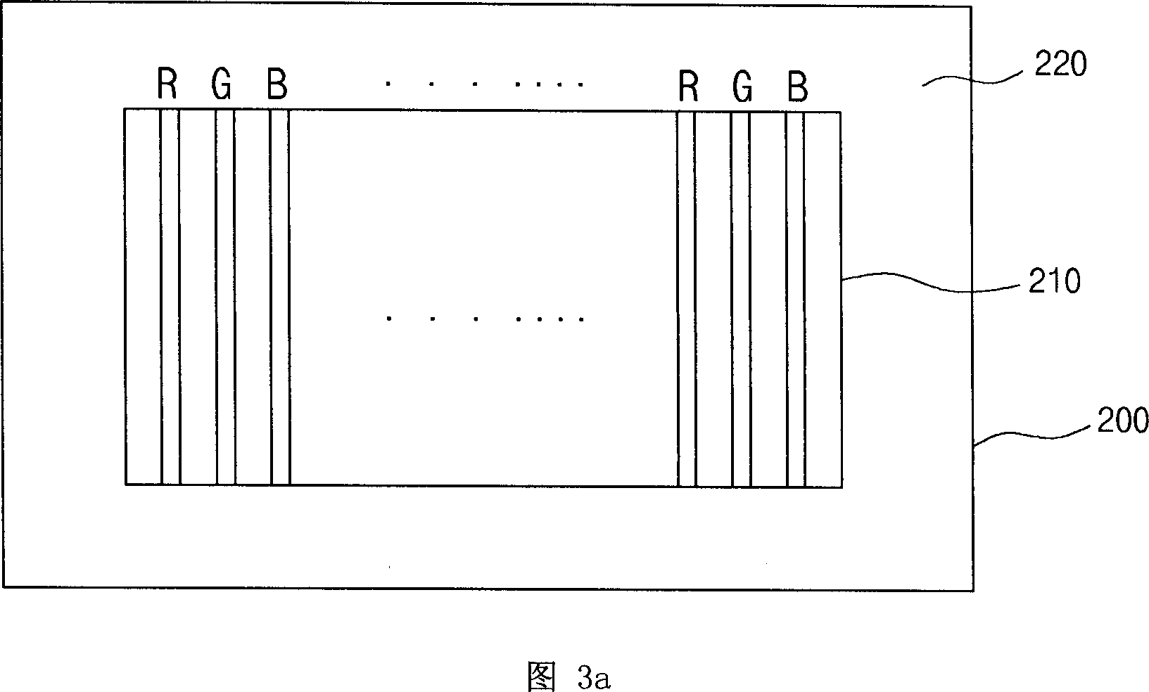
[0037] Figure 5 shows the position where the Align Mark is formed.
[0038] As shown in FIG. 5, the Align Mark according to the present invention is formed on the non-printing area 510 of the substrate 500 coated with the photosensitive film. Here, the photosensitive film is preferably composed of an indium oxide film ITO and Indium Tin Oxide.
[0039] At this time, more than one inscribed Align Mark is formed in the non-printing area, such as the symbols B, C, D, and E.
[0040] According to the present invention, the specific method of forming the Align Mark in the non-printing area 510 is shown in FIG. 6.
[0041] 6 is a schematic diagram of a method for forming an Align Mark of a plasma display panel according to the present invention.
[0042] As shown in FIG. 6, the Align Mark forming method of the plasma display panel according to the present invention is to form at least on
PUM
 Abstract
Description
Claims
Application Information
 - R&D Engineer
- R&D Manager
- IP Professional
- Industry Leading Data Capabilities
- Powerful AI technology
- Patent DNA Extraction
Browse by: Latest US Patents, China's latest patents, Technical Efficacy Thesaurus, Application Domain, Technology Topic.
© 2024 PatSnap. All rights reserved.Legal|Privacy policy|Modern Slavery Act Transparency Statement|Sitemap