Liquid crystal display device
a technology of liquid crystal display panel and manufacturing method, which is applied in the direction of thin material processing, instruments, chemistry apparatus and processes, etc., can solve the problems of lowering the manufacturing yield rate, the manufacturing yield, and the push up of the manufacturing cost of the liquid crystal display panel, so as to reduce the manufacturing yield rate and reduce the manufacturing cost. , the effect of easy correction
- Summary
- Abstract
- Description
- Claims
- Application Information
AI Technical Summary
Benefits of technology
Problems solved by technology
Method used
Image

Examples
embodiment 2
[0110]FIG. 8 is a schematic plan view showing the schematic constitution of a liquid crystal display panel according to a second embodiment of the present invention.
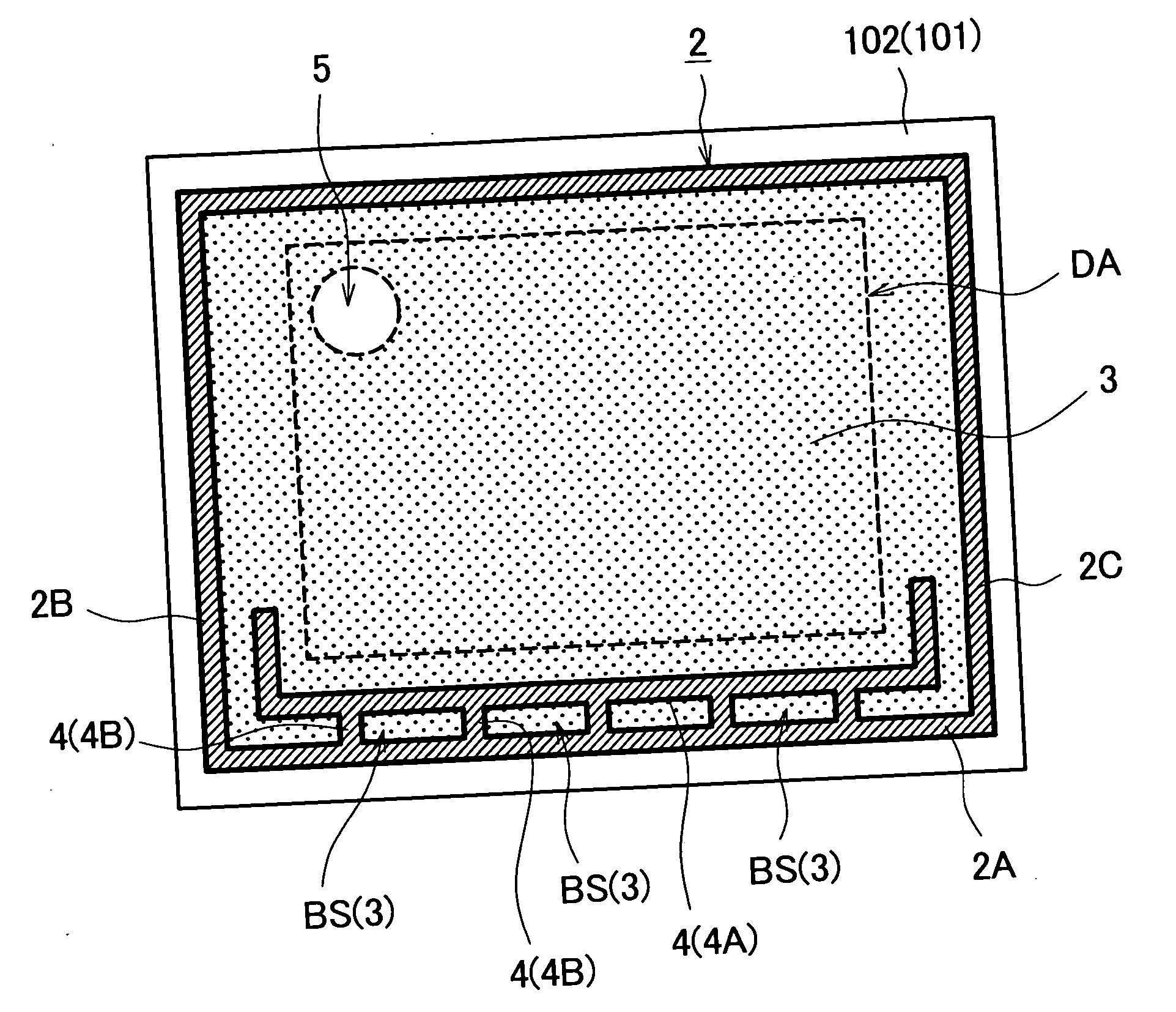
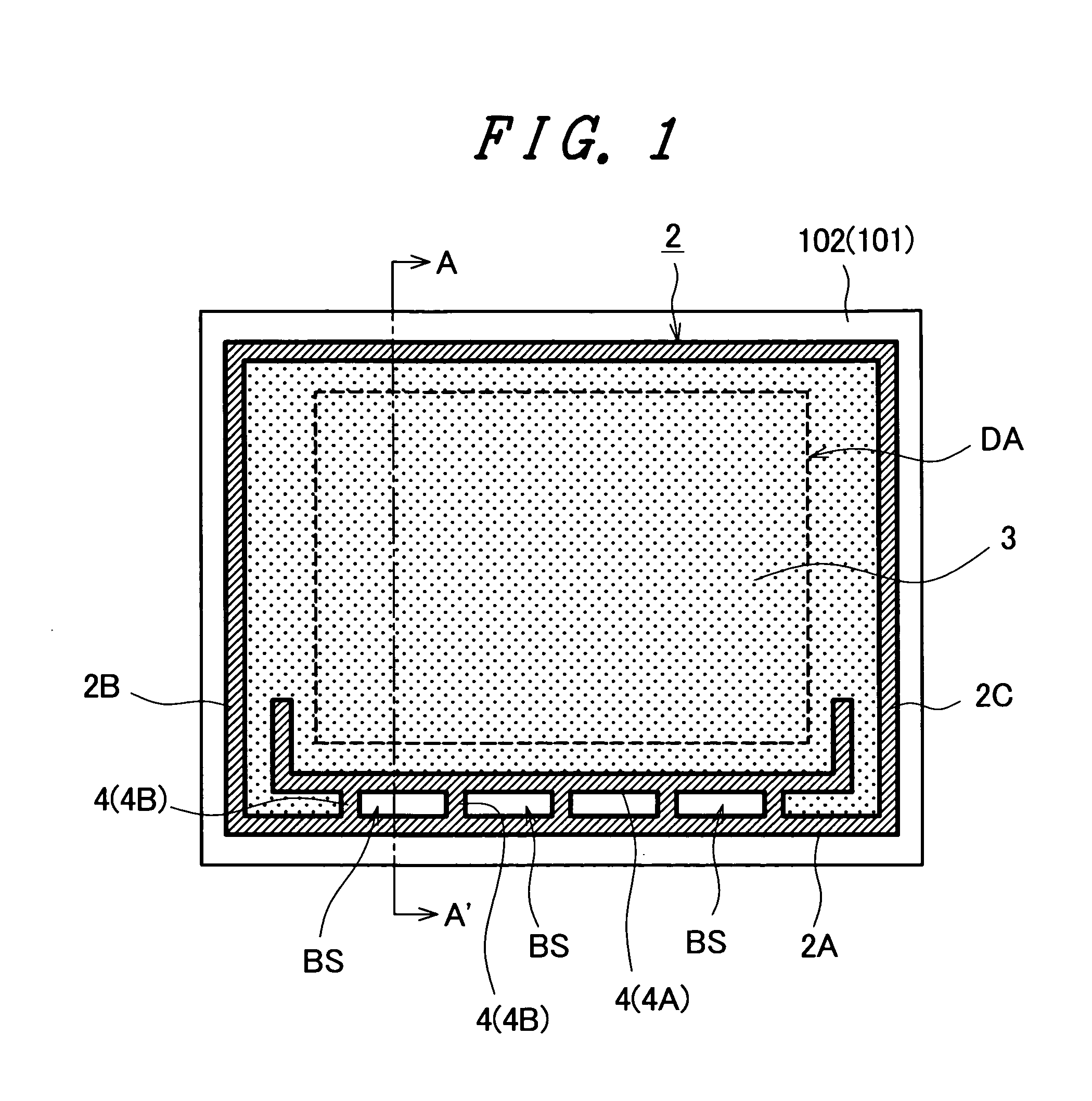
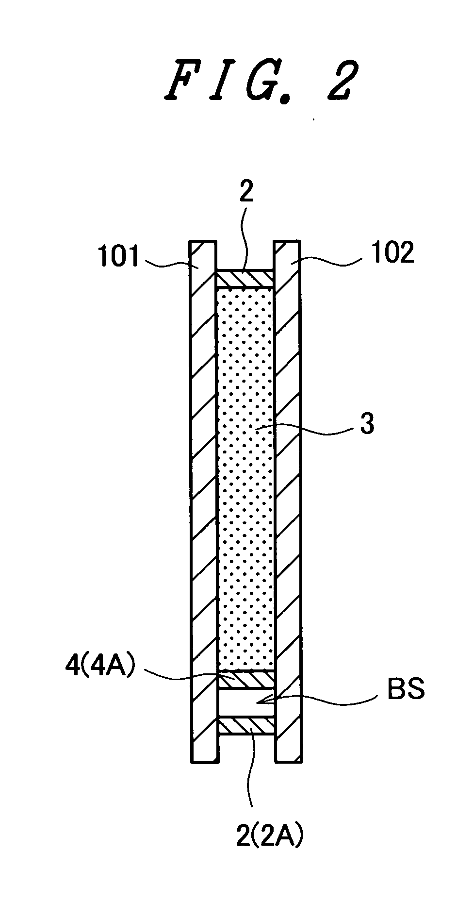
[0111] The liquid crystal display pane of this embodiment 2 includes, for example, as shown in FIG. 8, two substrates consisting of a first substrate 101 and a second substrate 102, an annular sealing material2 which separates a space defined between two substrates 101, 102 and a space outside the substrates 101, 102, a liquid crystal material 3 which is sealed in the inside of a space which is surrounded by two substrates 101, 102 and a sealing material 2, and a partition member 4 which forms one or more second regions BS in the inside of the space which is surrounded by two substrates 101, 102, and the sealing material 2 and outside an image display region DA. Here, the second region BS is, originally, in the same manner as the liquid crystal display panel of this embodiment 1, formed spatially separately and independent
embodiment 3
[0137]FIG. 11 is a schematic plan view showing the schematic constitution of a liquid crystal display panel according to a third embodiment of the present invention.
[0138] In the above-mentioned embodiment 1, the explanation is made with respect to the constitutional example of the liquid crystal display panel which can easily perform the correction of the defect when the defect which is referred to as gravitational shift occurs. On the other hand, in the above-mentioned embodiment 2, the explanation is made with respect to the constitutional example of the liquid crystal display panel which can easily perform the correction of the defect when the air bubbles are generated or the defect which is referred to as wipe displacement occurs. However, in actually manufacturing the liquid crystal display panel, until two substrates 101, 102 are adhered to each other using the sealing material 2 and, thereafter, the liquid crystal material 3 is filled in the space defined between two substrate
PUM
 Abstract
Description
Claims
Application Information
 - R&D Engineer
- R&D Manager
- IP Professional
- Industry Leading Data Capabilities
- Powerful AI technology
- Patent DNA Extraction
Browse by: Latest US Patents, China's latest patents, Technical Efficacy Thesaurus, Application Domain, Technology Topic.
© 2024 PatSnap. All rights reserved.Legal|Privacy policy|Modern Slavery Act Transparency Statement|Sitemap