Method of fabricating microphone device and thermal oxide layer and low-stress structural layer thereof

a technology of thermal oxide layer and microphone device, which is applied in the direction of electrostatic transducer microphone, microelectromechanical system, electrical transducer, etc., can solve the problems of mediocre physical characteristics of the deposited oxide layer b>12/b>, and the need for extremely long time to thermally form the oxide layer of several micrometers thick,

Inactive Publication Date: 2007-03-22
TOUCH MICRO SYST TECH
View PDF3 Cites 5 Cited by
  • Summary
  • Abstract
  • Description
  • Claims
  • Application Information

AI Technical Summary

Benefits of technology

This patented technology provides a way to make a structure with less stresses than previously possible without compromising its strength or durability. It involves creating two layers of material separately beforehand, which can be done by adding different materials at specific locations during the manufacturing process. By doing this, it becomes easier to control how well these structures work when they're used for their intended purpose.

Problems solved by technology

The technical problem addressed in this patent is improving the performance and efficiency of capacitive microelectronic devices used for detecting sounds caused by external sources such as loudspeakers or other acoustic equipment. Specifically, traditional methods involving depositing layers onto the surface of the structure can lead to poor quality and lower yields. To address these issues, new methods like thermal evaporation and plasma etching were developed. These methods improve the accuracy and resolution of the resulting structures but they also increase manufacturing costs.

Method used


Image

  • Method of fabricating microphone device and thermal oxide layer and low-stress structural layer thereof
  • Method of fabricating microphone device and thermal oxide layer and low-stress structural layer thereof
  • Method of fabricating microphone device and thermal oxide layer and low-stress structural layer thereof

Examples


Embodiment Construction

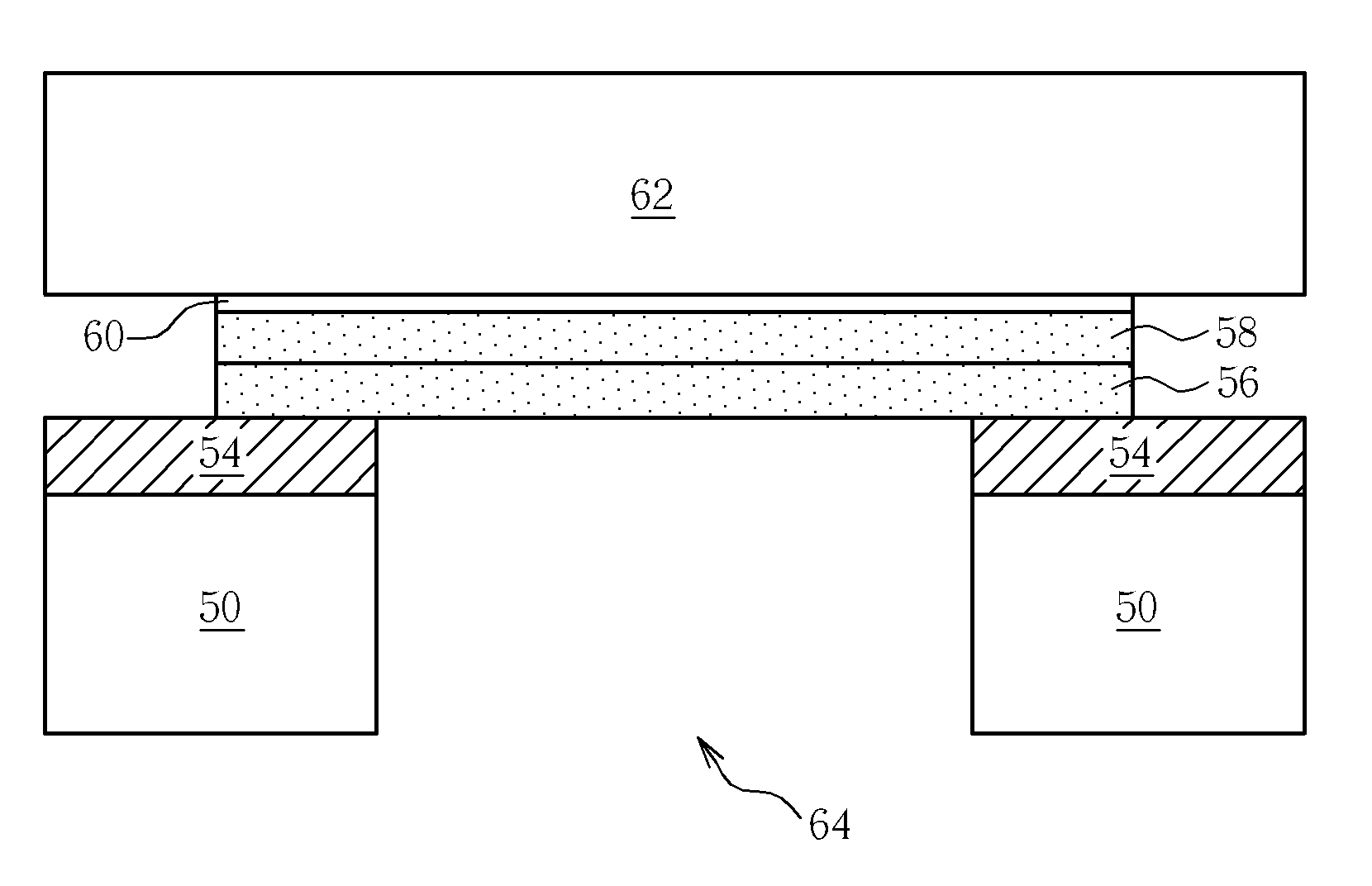
[0016] Referring to FIG. 7 to FIG. 15, FIG. 7 to FIG. 15 are schematic diagrams illustrating a method of fabricating a microphone device in accordance with a preferred embodiment of the present invention. It is appreciated that FIG. 7 to FIG. 15 only illustrate one microphone device, and the fabrication of microphone device may be divided into three stages: the first stage is to form a thermal oxide layer (illustrated in FIG. 7 to FIG. 9); the second stage is to form a structural layer (illustrated in FIG. 10 to FIG. 13); and the third stage is to form a back chamber (illustrated in FIG. 14 and FIG. 15).

[0017] As shown in FIG. 7, a substrate 50 e.g. a silicon wafer or an SOI wafer is provided. Subsequently, a plurality of trenches 52 are formed in the front surface of the substrate 50 by deep etching techniques such as inductively coupled plasma reactive ion etching (ICPRIE), deep X ray lithography, or electron cyclotron resonance (ECR) plasma etching. In this embodiment, the line wid


PUM


Abstract

A substrate is provided and a plurality of trenches are formed in the front surface of the substrate. Then, a thermal oxide layer is formed on inner walls of the trenches and the front surface of the substrate. Subsequently, a first structural layer is formed on the thermal oxide layer, dopants are implanted into the first structural layer, a second structural layer is formed on the first structural layer, and an annealing process is performed to reduce the stress of the first and second structural layers. Following that, the first and second structural layers are patterned to form diaphragms. Finally, the second structural layer is mounted on a support wafer with a bonding layer, and the back surface of the substrate is etched by deep etching techniques to form back chambers corresponding to the diaphragms. Each back chamber has a vertical sidewall and partially exposes the first structural layer.

Description


Claims


Application Information

Patent Timeline
Owner TOUCH MICRO SYST TECH
Why Eureka
Try Eureka