Signal analysis system and calibration method for multiple signal probes

Active Publication Date: 2008-02-28
TEKTRONIX INC
View PDF38 Cites 33 Cited by
  • Summary
  • Abstract
  • Description
  • Claims
  • Application Information

AI Technical Summary

Benefits of technology

[0004]These and other deficiencies of the prior art are addressed by the present invention of a system, apparatus and method for reducing measurement errors due to, for example, probe tip loading of a device under test and transmissions errors in a signal path containing the device under test. Briefly, the invention provides a method to calibrate one or more signal paths of a signal analysis system so that loading and through effects of signal analysis system are substantially removed from the signal analysis system measurements. As a result, the user will see a time domain display that represents the signal in a circuit under test as it would appear before the signal analysis system is attached to the circuit.

Problems solved by technology

This drop in impedance as frequency increases, coupled with the fact that many circuits being probed have a relatively low output impedance in the range of 25-150 ohms, results in a significant loading of the circuit under test by the probe.
As such, an acquired waveform received via a probe loading such a circuit may not accurately represent the voltage of the circuit prior to the introduction of the probe.
When more than one probe is coupled to the device under test, each probe may contribute to the loading of the device under test resulting in an inaccurate representation of the voltage of the circuit prior to the introduction of the probes.

Method used


Image

  • Signal analysis system and calibration method for multiple signal probes
  • Signal analysis system and calibration method for multiple signal probes
  • Signal analysis system and calibration method for multiple signal probes

Examples


Example

[0026]To facilitate understanding, identical reference numerals have been used, where possible, to designate identical elements that are common to the figures.

DETAILED DESCRIPTION OF THE INVENTION

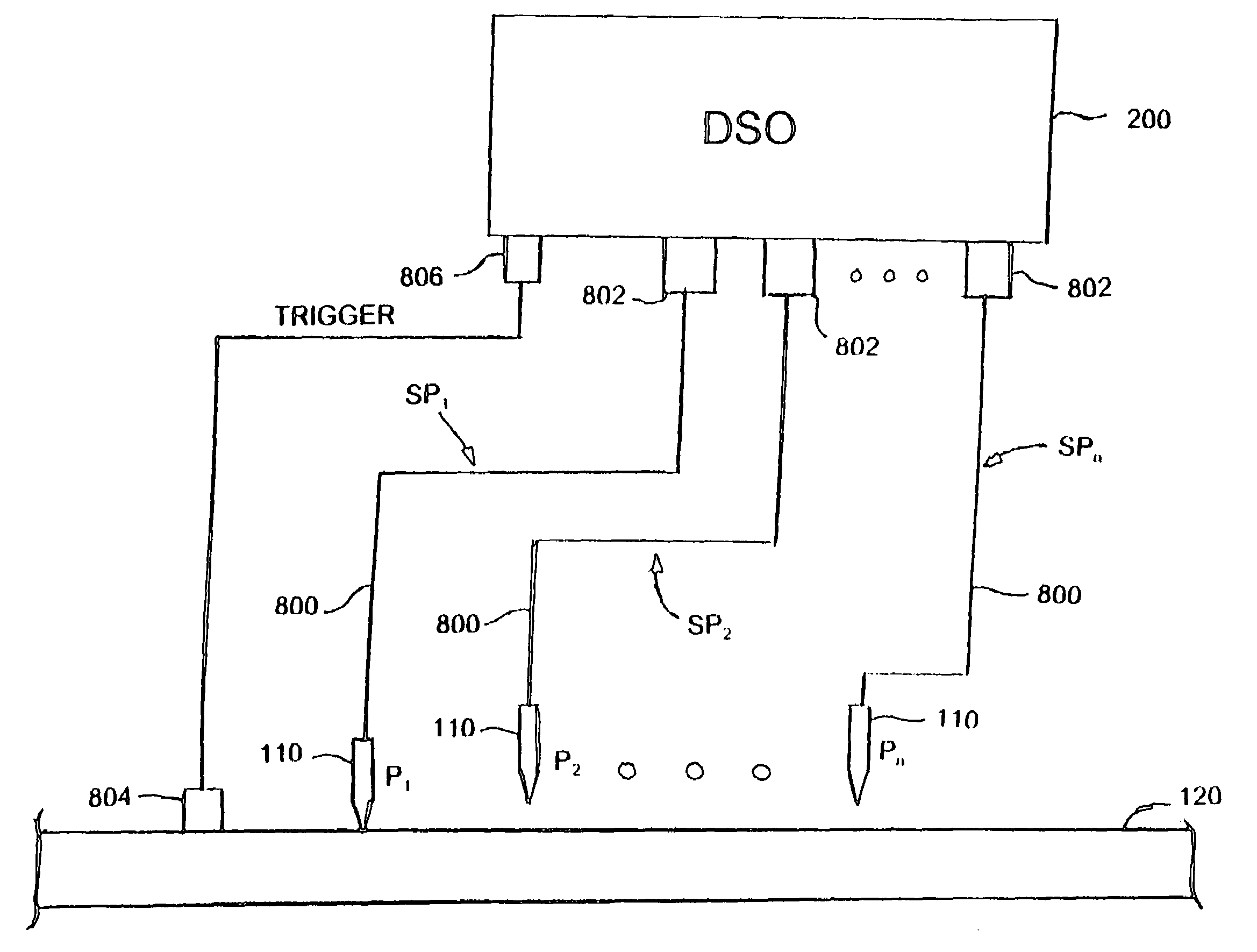
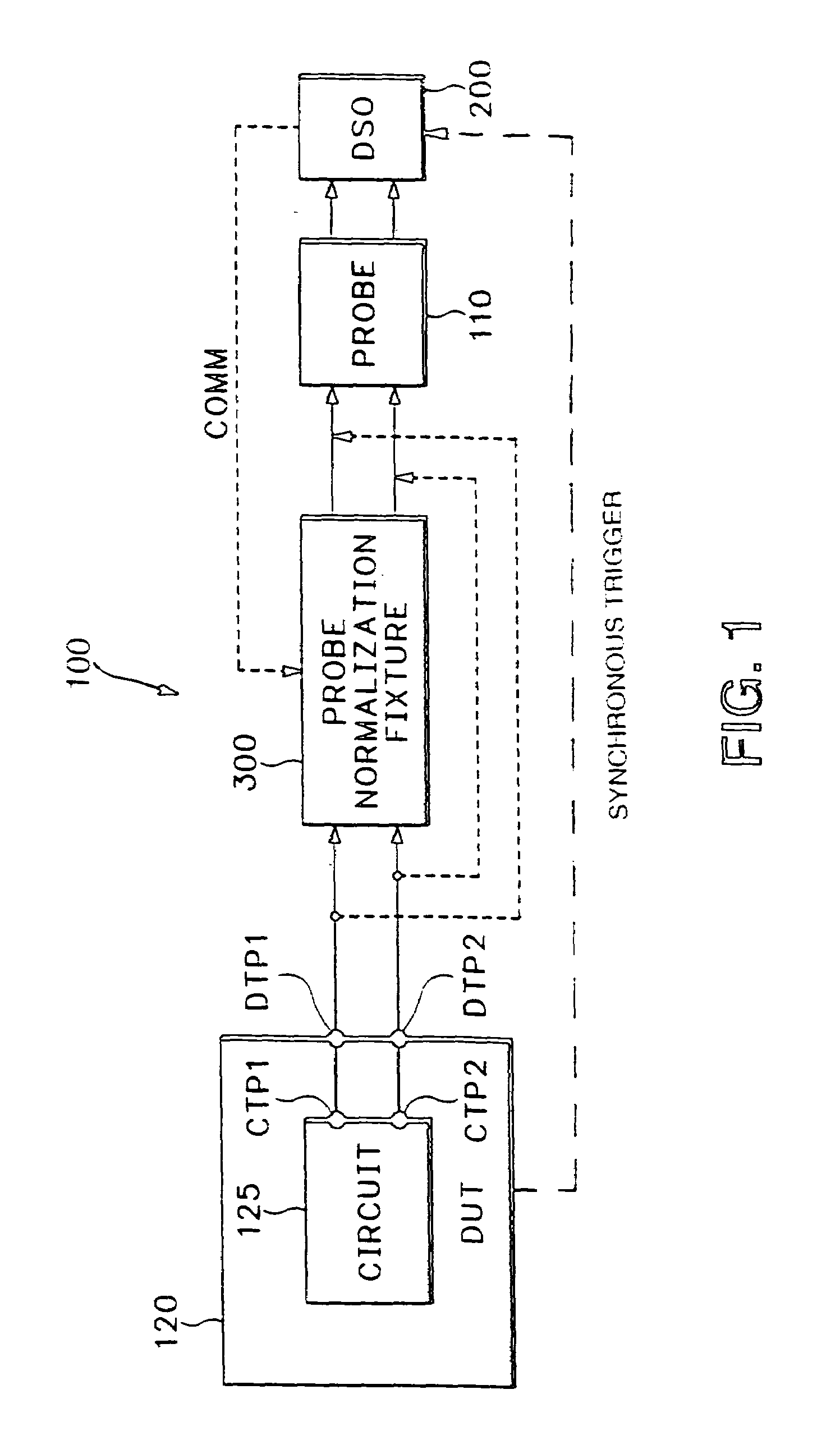
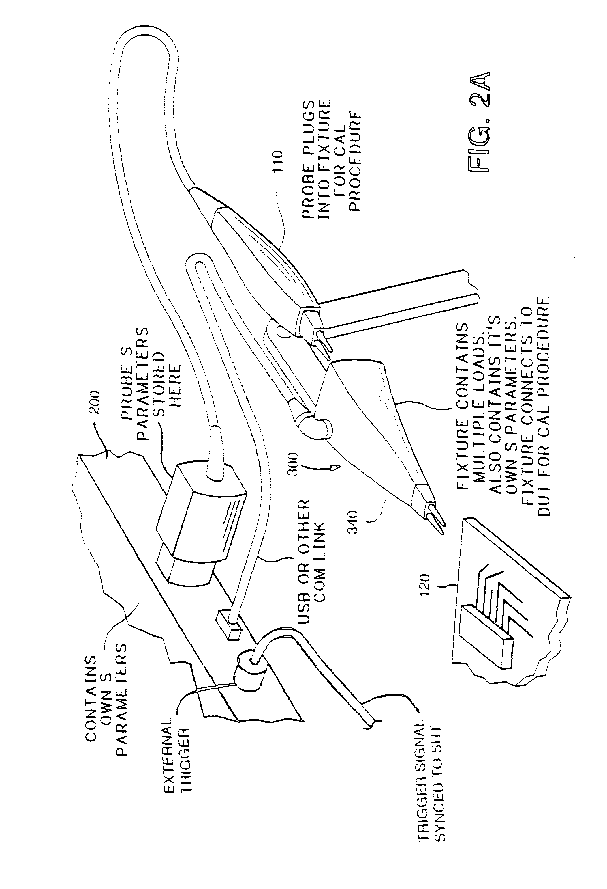
[0027]FIG. 1 depicts a high level block diagram of a signal analysis testing system 100 including a device under test arranged in accordance with various embodiments of the present invention. Specifically, a probe 110 is operably coupled to a signal analysis device such as a digital storage oscilloscope (DSO) 200 to provide thereto a signal under test (SUT) received from a device under test (DUT) 120. A probe normalization fixture 300 is selectively interposed between the DUT 120 and probe 110.

[0028]The invention operates to calibrate a signal path including the probe 110 and, optionally, DSO input channel to remove (i.e., de-embed) their respective signal degrading effects from the measurement of the DUT (or circuit) including transmission errors in the system. This de-embedding process is co


PUM


Abstract

A method and apparatus adapted to calibrate signal path of a signal analysis system such that loading effects of additional probes are substantially removed from the measurement. A signal under test from a device under test is coupled to a test probe and used with selectable impedance loads in the test probe to acquires sets of samples for characterizing transfer parameters of the device under test and compute open circuit voltages at the test probe. Other probes are coupled to the device under test and a set of measurement samples are acquired via the test probe. An equalization filter in either the frequency or time domain is computed from the open circuit voltage and measurement samples for reducing signal errors attributable to the measurement loading of the device under test by the test probe and other probes.

Description


Claims


Application Information

Patent Timeline
Owner TEKTRONIX INC
Why Eureka
Try Eureka