Circuit measuring operating speed and related semiconductor memory device

a technology of operating speed and semiconductor memory chip, which is applied in the direction of instruments, nuclear elements, nuclear engineering, etc., can solve the problems of inability to conduct direct operating speed measurements, inability to generate test signals at a sufficiently high frequency, and inability of test devices to accurately measure the operating speed of constituent semiconductor memory chips. , to achieve the effect of accurately measuring the operating speed of the constituent semiconductor memory chip

Inactive Publication Date: 2008-08-28
SAMSUNG ELECTRONICS CO LTD
View PDF6 Cites 3 Cited by
  • Summary
  • Abstract
  • Description
  • Claims
  • Application Information

AI Technical Summary

Benefits of technology

The present invention provides an improved way to measure how fast a semiconductor memory chip operates. This helps improve its performance and efficiency.

Problems solved by technology

The technical problem addressed in this patent is how accurately determine the operating speed of modern electronic devices without requiring expensive and bulky external measuring circuits. Current methods involve measuring the operating speed of each component separately, but these techniques require a larger amount of space and consume power. Therefore, there is a need for a more compact and cost-effective way to measure the operating speed of current electronic devices.

Method used


Image

  • Circuit measuring operating speed and related semiconductor memory device
  • Circuit measuring operating speed and related semiconductor memory device
  • Circuit measuring operating speed and related semiconductor memory device

Examples


Embodiment Construction

[0022]Embodiments of the invention will now be described more fully with reference to the accompanying drawings. The invention may, however, be embodied in different forms and should not be construed as limited to only the illustrated embodiments. Rather, these embodiments are presented as teaching examples. In the drawings, certain geometric relationships may be exaggerated for clarity. Throughout the drawings and written description like reference numbers and legends refer to like or similar elements.

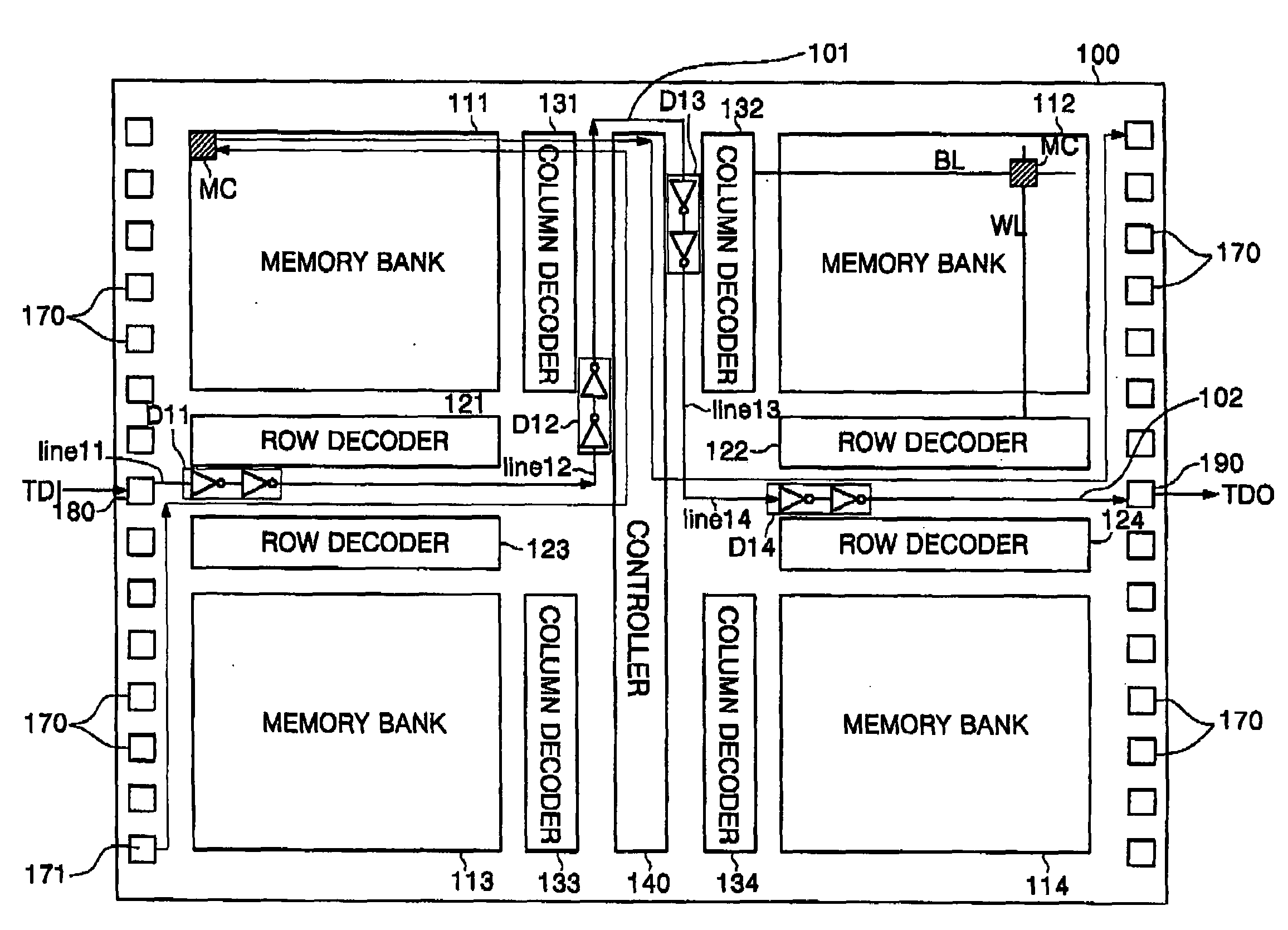
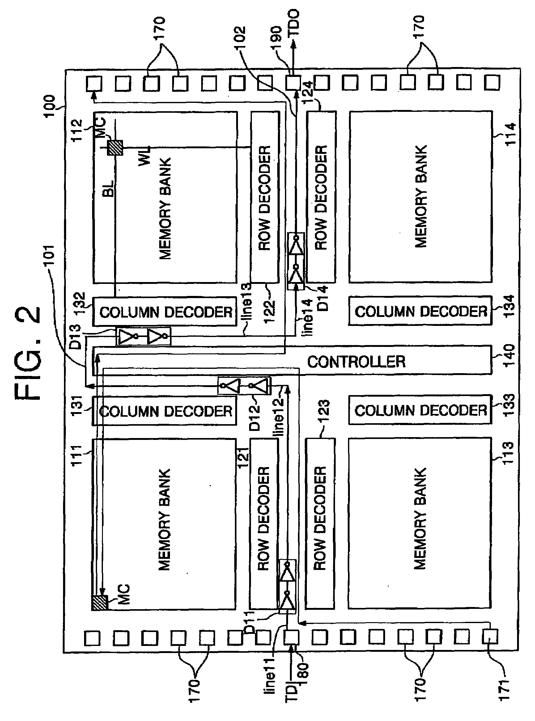
[0023]FIG. 2 is a schematic diagram illustrating a semiconductor memory chip incorporating a measuring circuit according to an embodiment of the invention. The term “chip” is used to denote a wafer level arrangement of circuits functionally enabling at least the read / write operations of the ultimately formed semiconductor memory device. Thus, a semiconductor memory chip is a wafer level fabrication of a wafer portion capable of being testing for operating speed and subsequently removed


PUM


Abstract

A circuit measuring the operating speed of a semiconductor memory chip in relation to a defined asynchronous access time is disclosed. The circuit includes a test signal path extending between a test input pad and a test output pad and is formed by a plurality of test signal path segments and at least one delay element associated with at least one of the plurality of test signal path segments, such that a delay time for a test signal communicated through the test signal path is indicative of the actual asynchronous access time for the semiconductor memory chip. Each one of the plurality of test signal path segments is either an interior test signal path segment or an exterior test signal path segment.

Description


Claims


Application Information

Patent Timeline
Owner SAMSUNG ELECTRONICS CO LTD
Why Eureka
Try Eureka