Semiconductor structure with improved capacitance of bit line
a technology of semiconductor and bit line, which is applied in the direction of bulk negative resistance effect devices, basic electric elements, electric devices, etc., can solve the problems of increasing delay in transmitting bit signals, so as to avoid high improve the capacitance of bit lines, and improve the effect of signal delay
- Summary
- Abstract
- Description
- Claims
- Application Information
AI Technical Summary
Benefits of technology
Problems solved by technology
Method used
Image

Examples
first embodiment
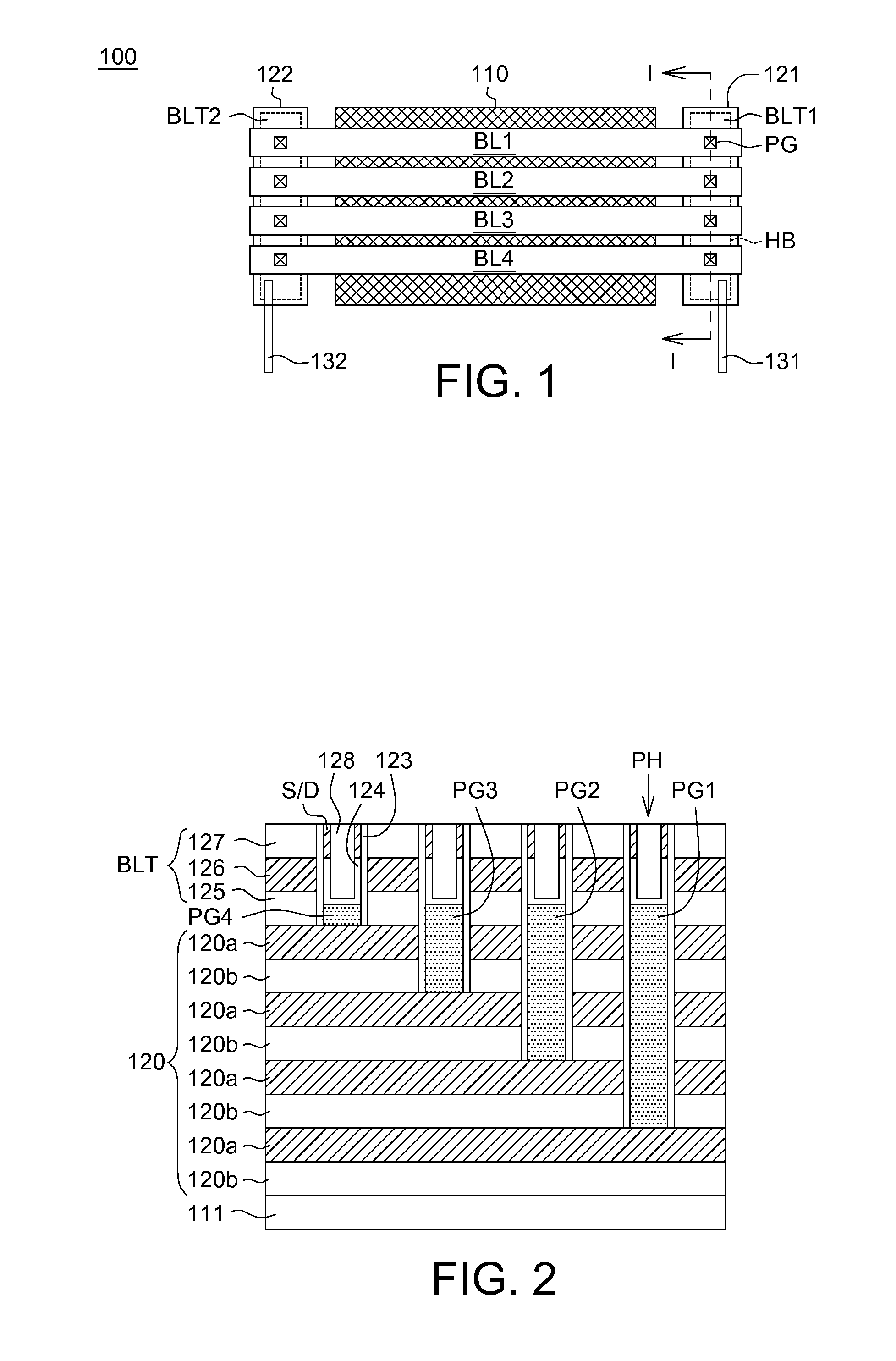
[0021]Referring to FIG. 1, a top schematic view of a semiconductor structure 100 with improved capacitance of bit lines according to an embodiment of the invention is shown. Taken four bit lines BL1-BL4 arranged in order for example, a stacked memory structure 110 is located between a first stair contact structure 121 and a second stair contact structure 122. The stacked memory structure 110, for example 3D NAND flash memory, has multi-layers of memory planes arranged from bottom to top in order. A first bit line BL1 is connected to a first layer of memory plane via the first stair contact structure 121, and a second bit line BL2 is connected to a second layer of memory plane via the first stair contact structure 121, and so on. Similarly, various bit lines BL1-BL4 can be connected to different memory planes via the second stair contact structure 122. In an embodiment, the first stair contact structure 121 and the second stair contact structure 122 are connected to the first conductive
second embodiment
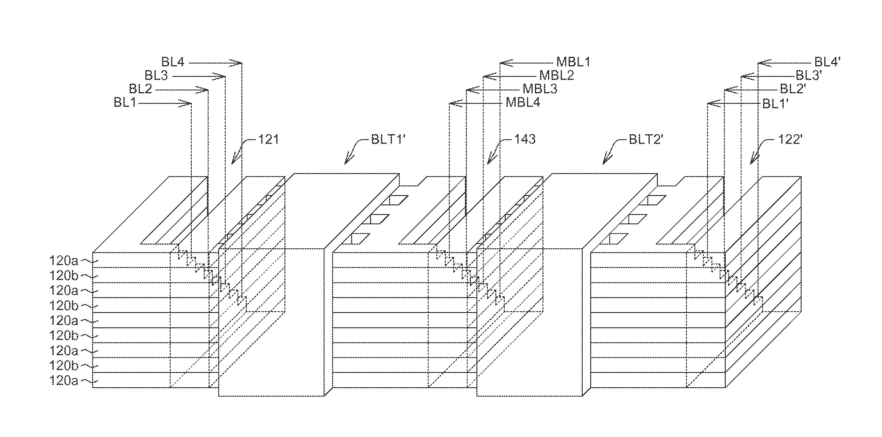
[0032]Referring to FIG. 7, a top schematic view of a semiconductor structure 101 with improved capacitance of bit lines according to another embodiment of the invention is shown. In the above embodiment, a group of transistor structures BLT is formed on the top of the stair contact structure 120, while a group of transistor structures BLT1′ (BLT2′) formed on a side of the stair contact structure 121 (122′) and a conductive line 131′ (132′) connected to the gate of the group of transistor structures BLT1′ (BLT2′) are disclosed in the present embodiment. The conductive line input a voltage to selectively open or close the transistor structures BLT1′ (BLT2′). The details of description of the bit lines BL1-BL4 (BL1′-BL4′), the first stair contact structure s 121 (121′), the second stair contact structure s 122 (122′) and the stacked memory structure 110 (110′) are similar to the structures disclosed in the first embodiment, and do not repeat again.
[0033]Referring to FIG. 8, the first stai
PUM
 Abstract
Description
Claims
Application Information
 - R&D Engineer
- R&D Manager
- IP Professional
- Industry Leading Data Capabilities
- Powerful AI technology
- Patent DNA Extraction
Browse by: Latest US Patents, China's latest patents, Technical Efficacy Thesaurus, Application Domain, Technology Topic.
© 2024 PatSnap. All rights reserved.Legal|Privacy policy|Modern Slavery Act Transparency Statement|Sitemap